Code:
D-04 Subject:
ENGINEERING MATERIALS
Time: 3
Hours
Max. Marks: 100
NOTE: There are 11
Questions in all.
· Question 1 is compulsory
and carries 16 marks. Answer to Q. 1. must be written in the space provided for
it in the answer book supplied and nowhere else.
·
Answer
any THREE Questions each from Part I and Part II. Each of these questions
carries 14 marks.
·
Any
required data not explicitly given, may be suitably assumed and stated.
Q.1
Choose the correct or best alternative in the following: (2x8)
a. Materials, which provide
a path to the magnetic flux, are classified as
(A) insulating materials. (B)
semi conducting materials.
(C)
magnetic materials. (D) dielectric
materials.
b. Germanium possesses
(A) one valence electrons. (B)
two valence electrons.
(C) three valence electrons. (D)
four valence electrons.
c. Dielectric
constant of vacuum is
(A) infinity. (B)
100.
(C) one. (D)
zero.
d. Ferrites are
(A) ferromagnetic material. (B)
ferrimagnetic materials.
(C) anti ferromagnetic material. (D)
diamagnetic materials.
e. Thermocouples
are used for measuring
(A) current. (B)
voltage.
(C)
temperature. (D) pressure.
f. The relative permeability of
a paramagnetic substance is
(A) unity. (B)
slightly more than unity.
(C) zero. (D) less
than unity.
g. Hall
effect may be used for which of the following?
(A) determining whether the
semiconductor is p or n type.
(B) determining the carrier
concentration.
(C) calculating the mobility.
(D) All the above.
h. Manganin
is an alloy of
(A)
copper, manganese and nickel. (B) copper and manganese.
(C)
manganese and nickel. (D) manganese, aluminium
and nickel.
PART I
Answer any THREE Questions. Each
question carries 14 marks.
Q.2 a. Explain
the factors which change the resistivity of a conducting material (8)
b. A
heater element is made of nichrome wire having resistivity equal to  ohm-m. The
diameter of the wire is 0.4mm. Calculate the length of the wire required to
get a resistance of 40
ohm-m. The
diameter of the wire is 0.4mm. Calculate the length of the wire required to
get a resistance of 40  . (6)
. (6)
Q.3 a. Explain
superconductivity and explain the effect of magnetic field on superconductors. (6)
b. Give the properties and
application of copper and aluminium. (8)
Q.4 a. What
is polarisation? Explain. (6)
b. Give
the properties and application of glass and cotton. (8)
Q.5 a. Give
the names of four alloys along with their composition, which are used for
making heater and thermocouple elements. (6)
b. Explain
ferroelectricity and piezoelectricity. (8)
Q.6 a. Explain the electrical contact materials with examples. (7)
b. Explain the terms dielectric constant and dielectric
loss angle. (7)
PART II
Answer any THREE Questions. Each
question carries 14 marks.
Q.7 a. Explain
the effect of temperature on the conductivity of a semiconductor. (8)
b. Explain n-type and
p-type semiconductors. (6)
Q.8 Differentiate
between diamagnetic, paramagnetic, ferromagnetic and ferrimagnetic materials
and give examples of each. (14)
Q.9 a. Give
the properties and uses of silicon iron alloy and nickel iron alloy. (6)
b. Explain the working
of an npn transistor. (8)
Q.10 a. What is meant
by doping? How does it affect a semiconductor? (6)
b. Explain the factors
affecting permeability and hysterisis loss. (8)
Q.11 Write notes on
(i)
Classification
of materials on the basis of energy band. (7)
(ii)
Germanium
and silicon. (7)
Detailed
Solutions D - 04 DEC 2004
|
|
1.
a. C Magnetic materials.
b. D
Four valence electrons.
c. C
One.
d. B
Ferrimagnetic materials.
e. C
Temperatures.
f. B
Slightly more than unity.
g. D
Determining whether the semiconductor is p or n type, determining the
carrier concentration, calculating the mobility.
h. A Copper, manganese and nickel.
PART- I
2a) Factors, which
change the resistivity of conducting materials: -
Temperature- The electrical
resistance of most metals increases with increase of temperature while those
of semiconductors and electrolytes decreases with increase of temperature.
Alloying- Alloying is
another factor, which affects the resistivity of a material. By the addition of
some impurity to a metal, its resistivity can be changed. Alloys have higher
resistivity than that of pure metal.
;’Mechanical
stressing-When a material undergoes a mechanical treatment, its resistivity
changes due to mechanical distortion of the crystal structure.
Age Hardening- Age hardening
increases the resistivity of an alloy.
2b) When the heater element is Nichrome r = 100x 10-8
W-m.
 a = p (0.4 x10⁻³)2
m2
a = p (0.4 x10⁻³)2
m2
4
a = 12.6 x 10⁻⁸ m2
R = 40W

 R = r l or 40 = 100 x 10-8 x l
a
12.6 x 10⁻⁸
l = 5.04 m.
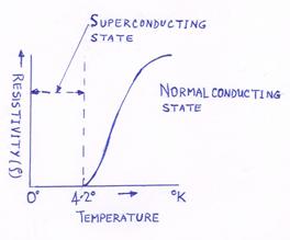
3a) A
large number of metals become superconducting below a temperature, which is
the characteristic of the particular metal. They have zero resistivity and
the temperature at which this change takes place is called superconducting
transistion temperature. Metals, which are good conductors at room temperature
like gold, silver, tin, do not exhibit superconducting properties. Whereas
metals and compounds which have superconducting properties at certain
temperatures are insulators at room temperature.
It is possible to
destroy superconductivity by the application of a strong magnetic field. When,
the magnetic field exceeds a certain critical value, the superconducting state
disappears, the magnetic field penetrates the material and electrical
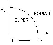
resistance is restored. In fig.(b) Hc is the critical magnetic field
and TC critical temperature.
3b) Copper: Properties
1) It is reddish brown
in color.
2) It is malleable and
ductile and can be cast, forged, rolled, drawn and machined.
3) It melts at 10830C.
4) It easily alloys
with other metals.
5) Electrical
resistivity of copper is 1.7x10⁻⁸ W-m.
6) Tensile strength
for copper is 210 MN/m2.
7) It is highly resistant
to corrosion.
8) It is a
non-magnetic material.
Applications: - Copper is used in conductor wires, coil windings of
generators and transformers, cables, busbars etc. Alloys of copper (like Brass,
Bronze, Constantan, Manganin etc) are very useful for different purposes.
Aluminium: Properties
1) Pure aluminium is
silver white in color.
2) It is a ductile
metal and can be put to a shape by rolling, drawing and forging.
3) It melts at 6550C.
4) It is resistant to
corrosion.
5) Its tensile
strength is 60MN/m2.
6) It can be alloyed
with other elements.
7) Annealing can
soften it.
8) It has a higher
thermal conductivity.
Applications:- Aluminium is widely
used as conductor for power transmission and distribution. It is used in
overhead transmission lines, busbars, ACSR conductors etc.
4a)
When a dielectric material (polar) is subjected to an electric field the
dipoles of the material get oriented into a particular direction under the
effect of the electric field. The material is said to be polarized and the
phenomenon as polarization. In case of non polar material, the atoms or
molecules get polarized and induces dipole moments at atomic level. The
individual dipoles get oriented towards field direction The dipole moment (p)
per unit volume is called polarization (p). The dipole moment is proportional
to the local electric field and the constant of proportionality is called
polarizability. There are three types of polarzation / polarizability-
1. Electronic or
atomic polarization
2. Oriental or dipolar
polarization
3. Ionic polarization.
4b) Glass:
- It is an amorphous substance. It consists of silicates and in some cases
borates and phosphates. Properties
1) It has high
resistivity & dielectric strength at ambient temperature.
2) Temperature
coefficient is –ve and very large.
3) Tensile strength is
low.
4) Coefficient of
thermal expansion considerably varies with composition.
5) It is susceptible
to destruction when used in high and low temperature cycle.
6) Surface resistivity
falls considerably when exposed to moisture.
Applications:- Moulded glass is
used in electrical bushings, fuse bodies, insulators. It is used as dielectric
in capacitors. It is used in the manufacture of radio and television tubes,
electrical lamps, and laminated boards. It is used to make optical fibers used
in optical communications.
Cotton:- This is base
material for insulating fibres. Properties of cotton can be improved by
Impregnating
with varnish. Properties
1) It is hygroscopic. Moisture
absorption is 70%.
2) It has low
dielectric strength.
3) Its resistivity
changes with moisture content.
4) It can be used upto
1100C.
5) Its density is
1.54gm/cm3.
Applications:- It is used as
insulating material for armature winding of small and medium sized machines,
small transformers, coils and chokes. Cotton covered wires are used for winding
of small magnet coils.
5a) Constantan or Eureka { (55-60%) Cu,
(45-40%)Ni}
German Silver (an alloy of Cu, Zn,
Ni)
Manganin (86% Cu, 2% Ni, 12% Mn)
Nichrome (61% Ni, 15% Cr, 24% Fe)
5b) Ferroelectricity:
- Ferroelectric materials have a high dielectric constant, which is
non-linear i.e., it depends to a considerable extent on the intensity of the
electric field. Such materials exhibit hysterisis loops, i.e. the polarization
is not a linear function of applied electric field. If the center of gravity of
the positive and negative charges in a body does not coincide in the absence of
an applied electric field, the substance has an electric dipole moment. It
contains small regions called ferroelectric domains and all dipoles are
parallely oriented in a domain but different domains are randomly oriented in
absence of external electric field. So the material is said to be spontaneously
polarized and called ferroelectric material. When the temperature exceeds a
certain value called the Curie point, the substance loses its ferroelectric
properties. Ex. Rochelle salt, Potassium dihydrogen phosphate, Barium titanate.
Piezoelectricity:- Piezoelectricity
provides us a means of converting electrical energy to mechanical energy
and vice versa.
When an
electric field is applied to a substance it becomes polarized, the electrons
and nuclei assume new geometric positions and the mechanical dimensions of the
substance are altered. This phenomenon is called electrostriction. The reverse
effect i.e. production of polarization by the application of mechanical
stresses can take place only if the lattice has no center of symmetry, this
phenomenon is known as piezoelectricity. Ex. Rochelle salt, Quartz, Barium
titanate.
6a) Electrical
contact materials: - A number of elements in their pure form such as
copper, molybdenum, nickel, palladium, platinum, silver and tungsten are mostly
acceptable make and break contact materials. Alloys of the above mentioned
elements are also used for electrical contacts. Silver is an important contact
material. Copper added to silver reduces the cost of the contact material.
Whereas a combination of tungsten and silver results in a contact material
having the advantages of the individual metals. A silver tungsten contact
material will have high thermal and electrical conductivity. Copper contacts
are used in control relays, motor starter switches and tap changers. Copper
contacts may be used for currents (a.c or d.c) upto 500A and voltages (a.c or
d.c) upto 600V. Contacts made of silver and silver alloys are widely used.
Silver has better resistance to oxidation compared to copper and can be used
for voltages (a.c or d.c) upto 600V and direct currents upto 50A and alternating
currents upto 200A. Such contacts are used in all types of industrial
applications, relays, generator cut outs, thermal overload devices and
thermostatic control.
6b) Dielectric Constant or Permittivity: - Every
insulating material possesses an electrical capacitance. The capacitance of
such unit depends upon dimensions and kind of dielectric placed between the
capacitor plates. The capacitance of a parallel plate capacitor may be
calculated from the formula C =Î A/t
where Î is the permittivity of the material
in F/m, A = Area of the plates and t = thickness of dielectric. Also Î= C/CO, where C is the capacity
in presence of dielectric and CO is the capacity in air or vacuum or
in the absence of dielectric.
Thus
permittivity Î of a material is a measurement of its ability to form an electrical
capacitance of the insulating material, the dimensions of the capacitor being
taken equal. Dielectric constant or permittivity is not a constant but varies
with temperature and frequency.
Dielectric
loss angle: - when an insulating material is subjected to alternating
voltage, some of the electric energy is absorbed by the insulation and is
dissipated as heat. Energy absorbed by the material in unit time is called
dielectric loss. A perfect dielectric has a current, which leads the voltage by
900, but the practical dielectric material has a current, which
leads the voltage by less than 900. The dielectric phase angle is q and d = 900 -
q is the dielectric
loss angle.
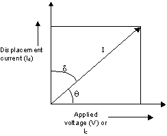
Also I
is the phasor sum of Id & Ic, where Ic is
the conduction current which is in phase with the applied voltage and Id
is the displacement current which is in quadriture phase with applied voltage.
PART- II
7a) The electrical conductivity of semiconductor changes
appreciably with temperature variations.
At absolute zero, it behaves as an insulator.
At room temperature, because of thermal energy, some of the covalent bonds of
the semiconductor break. The breaking of bonds sets those electrons free, which
are engaged in the formation of these bonds. This results in few free
electrons. These electrons constitute a small current if potential is applied
across the semiconductor crystal. This shows the conductivity for intrinsic
semiconductor increases with increase in temperature as given by h =A exp(-Eg/2kT) where h is the carrier concentration, Eg
is the band gap and T is the temperature and A is constant. In case of
extrinsic semiconductors, addition of small amount of impurities produces a
large number of charge carriers. This number is so large that the conductivity
of an extrinsic semiconductor is many times more than that of an intrinsic
semiconductor at room temperature. In n - type semiconductor all the donors
have donated their free electrons, at room temperature. The additional thermal
energy only serves to increase the thermally generated carriers. This increases
the minority carrier concentration. A temperature is reached when number of
covalent bonds that are broken is large, so that number of holes is
approximately equal to number of electrons. The extrinsic semiconductor then
behaves like intrinsic semiconductor.
7b) n – type semiconductor:- When small amount of
pentavalent impurity( group V elements) is added to a pure semiconductor
providing a large number of free electrons in it, the extrinsic semiconductor
thus formed is known as n- type semiconductor. The addition of pentavalent
impurities such as arsenic and antimony provide a large number of free
electrons in the semiconductor crystal. Such impurities, which produce n- type
semiconductors, are known as donor impurities because each atom of them donates
one free electron to conduction band in the semiconductor crystal.
p - type semiconductor:- When small amount of
trivalent impurity (group III elements) is added to a pure semiconductor
providing a large number of holes in it, the extrinsic semiconductor thus
formed is known as p- type semiconductor. The addition of trivalent impurities
such as gallium and indium provide a large number of holes in the semiconductor
crystal. Such impurities, which produce p- type semiconductors, are known as
acceptor impurities because each atom of them creates one hole, in valence
band, which can accept one electron.
8) Diamagnetic Materials:- These are the
materials whose atoms do not carry permanent magnetic dipoles. If an
external magnetic field is applied to a diamagnetic material, it induces a
magnetization in the direction opposite to the applied field intensity. For
these materials the relative permeability is negative. These are hardly used as
magnetic material in electrical/ electronic engineering applications. Example:
Aluminium oxide, copper, gold, barium chloride, superconductor
Paramagnetic Materials:- The
atoms of these materials contain permanent magnetic dipoles. Individual dipoles
are oriented in random fashion such that resultant magnetic field is zero or
negligible. For these materials relative permeability is slightly greater than
unity and it is independent of magnetizing force. Example: Chromium chloride,
chromium oxide, manganese sulphate, air. . In presence of external magnetic
field, paramagnetic materials get weakly magnetized in the field direction and
the susceptibility is given by c = C/T
where C is a curie constant and T is the temperature.
Ferromagnetic Materials:-
These are materials in which magnetic dipoles interact in such a manner that
they tend to line up in parallel. A ferromagnetic substance consists of a
number of small regions or domains, which are spontaneously magnetized. The
direction of magnetization varies from domain to domain. The resultant
magnetization is zero or nearly zero as the domains are randomly oriented. The
relative permeability is very high. The ferromagnetic materials are widely used
in industries. Example: Iron, nickel, cobalt. The susceptibility of these is
given by c= C/ T-TC where C
is Curie constant, TC is the Curie temperature above which the
ferromagnetic material exhibits paramagnetic behaviour.
Ferrimagnetic Materials:-These
are materials in which unequal magnetic dipoles are lined up antiparallel to
each other. The permeabilities are of the order that for ferromagnetic
materials under ordinary conditions. The magnetic characteristics of
ferrimagnetic materials are similar to those of ferromagnetic materials, as
they show spontaneous magnetization below a certain temperature. Example:
Magnetite, nickel, ferrite. The susceptibility of these is given by c= C/ T ±
q where C is Curie constant, T is the
temperature.
9a) Silicon Iron alloy:- Pure iron has low
resistivity, which results in higher eddy current losses. These losses can be
minimized by increasing the resistivity of the material, which is achieved by
adding 1 to 4 % of silicon to iron. Silicon increases the electrical
resistivity of iron. It reduces hysteresis loss. The magnetostriction effect is
also reduced. Silicon also improves resistance to corrosion and oxidation and
increases hardenability.
Silicon Iron alloy is used
in the form of thin sheets called laminations. These laminations are used in
transformers, small machines and large turbo- generators.
Nickel Iron alloy:- A
group of iron alloys containing between 40 to 90 % nickel have much
higher permeabilities at low flux densities and lower losses than ordinary
iron. The important alloys are permalloy and mumetal. Mumetal has lower
permeability but higher resistivity. Addition of small amounts of other
elements to nickel iron alloys improves their magnetic properties. Nickel
improves strength, toughness and resistance to fatigue. It also lowers the critical
cooling rate and hence increases hardenability.
Nickel Iron alloy is widely
used in transformer cores and loading coils for telephone circuits, instrument
transformers, for magnetic circuits of instruments, for magnetic screens of
electronic equipments.
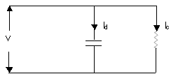
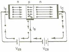
9b) Working of npn transistor:- An npn
transistor is shown in the fig. The emitter base junction is forward biased
while the collector base junction is reversed biased. The forward biased
voltage VEB is quite small, whereas the reverse biased voltage VCB
is considerably large.
As the emitter base junction is forward
biased, a large number of electrons (majority carrier) in the emitter (n-type
region) are pushed towards the base. This constitutes the emitter current IE.
When these electrons enter the p-type material (base), they tend to combine
with holes. Since the base is lightly doped and very thin, only a few electrons
(less than 5%) combine with the holes to constitute base current IB.
The remaining electrons (more than 95%) diffuse across the thin base region and
reach the collector space charge layer. These electrons then come under the
influence of positively biased n- region and are attracted or collected by the
collector. This constitutes the collector current IC. Thus, it is
seen that almost the entire emitter current flows into the collector circuit.
The emitter current is the sum of the collector, and base current. IE
=IC + IB.
10a)
Doping: - The process by which an impurity is added deliberately to a
semiconductor is known as doping. A semiconductor to which an impurity at
controlled rate is added to make it conductive as required is known as an
extrinsic semiconductor. The purpose of adding impurity in the semiconductor
crystal is to increase the number of free electrons or holes to make it more
conductive. If pentavalent impurity is added to a pure semiconductor a large
number of electrons will exist in it. If a trivalent impurity is added a large
number of holes will exist in the semiconductor.
10b) Factors
affecting permeability and hysterisis loss: - If the initial permeability
is high, the hysterisis loss is low and vice versa. The permeability and the
hysterisis loss depend upon the physical condition and chemical purity of the
sample. The crystals of a ferromagnetic material when cold worked experience
deformation as a result of which the material has very poor magnetic
properties. Due to the internal strains on the domains, greater magnetic field
is required to give a definite magnetization. Therefore the permeability
decreases and the hysterisis loss is increased. A material, which has suffered
magnetic damage due to cold work, may be heated to a sufficiently high
temperature when the magnetic properties will be restored. The highest
magnetic permeability and the lowest hysterisis loss that can be obtained are
limited by the impurity content of the materials. Impurities affect the regular
geometric pattern of the crystal and are harmful to the magnetic properties.
The main impurities in the magnetic materials used for transformer cores and
electrical machinery are carbon, sulphur, oxygen and nitrogen. Carbon is most
detrimental and the amount of carbon is kept to a low value of 0.01% in
commercial materials.
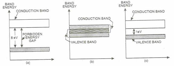
11a) Classification
of materials:- On the basis of energy band materials are classified as
insulators, conductors, semiconductors.
Insulators:- Substance like wood, glass, which do not allow the passage
of current through them are known as insulators. The valence band of these
substances is full whereas the conduction band is completely empty. The
forbidden energy gap between valence band and conduction band is very large
(8ev) as shown in fig. (a). Therefore a large amount of energy, i.e. a very
high electric field is required to push the valence electrons to the conduction
band. This is the reason, why such materials under ordinary conditions do not
conduct at all and are designated as insulators.
Conductors:- Substances like copper, aluminium, silver which allow the
passage of current through them are conductors. The valence band of these
substances overlaps the conduction band as shown in fig. (b). Due to this
overlapping, a large number of free electrons are available for conduction.
This is the reason, why a slight potential difference applied across them
causes a heavy flow of current through them.
Semiconductors:-
Substances like carbon, silicon , germanium whose electrical conductivity lies
in between the conductors and insulators are known as semiconductors. The
valence band of these substances is almost filled, but the conduction band is
almost empty. The forbidden energy gap between valence and conduction band is
very small (1ev) as shown in fig. ( c). Therefore comparatively a smaller
electric field is required to push the valence electrons to the conduction
band. This is the reason, why such materials under ordinary conditions do not
conduct current and behaves as an insulator. Even at room temperature, when
some heat energy is imparted to the valence electrons, a few of them cross over
to the conduction band imparting minor conductivity to the semiconductors. As
the temperature is increased, more valence electrons cross over to the
conduction band and the conductivity of the material increases. Thus these
materials have negative temperature co-efficient of resistance.
11b)
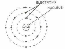
Germanium:- It is one of the most common semiconductor material used for
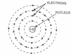
the application in electronics. The atomic number is 32. The number of
electrons in the first, second, third and fourth orbit are 2, 8, 18and 4. It is
clear that germanium atom has four valence electrons in the outermost orbit. It
is known as tetravalent element. The germanium atoms are held together through
covalent bonds. The forbidden gap in this material is very small 0.7ev. So
small energy is sufficient to lift the electrons from valence to conduction
band.
|
|
|
|
|
 |
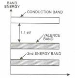
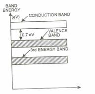
Silicon:- Silicon is another most commonly used semiconductor. Its
atomic number is 14. The number of electrons in first, second and third orbit
are 2, 8 and 4. The silicon atoms are also having four valence electrons and
are known as tetravalent element. The various silicon atoms are held together
through covalent bonds. The atoms of silicon are arranged in orderly pattern
and form a crystalline structure. The forbidden energy gap in this material is
quite small i.e. 1.1ev. It also needs small amount of energy to lift the
electrons from valence to conduction band.
Atomic structure of Silicon
|
|
Energy Band Diagram of Silicon