DipIETE – ET (NEW SCHEME) – Code: DE56
Subject: ANALOG ELECTRONICS
 Time: 3 Hours
Max. Marks: 100
Time: 3 Hours
Max. Marks: 100
NOTE: There are 9 Questions in all.
· Question 1 is compulsory and
carries 20 marks. Answer to Q.1 must be written in the space provided for it in
the answer book supplied and nowhere else.
· Out of the remaining EIGHT
Questions, answer any FIVE Questions. Each question carries 16 marks.
· Any required data not
explicitly given, may be suitably assumed and stated.
Q.1 Choose
the correct or the best alternative in the following: (2![]() 10)
10)
a.
Most commonly used technique for
preparing single crystal silicon from polycrystalline silicon is by __________.
(A)
(C) Czochralski method (D) None of the above
b. Diffusion of impurities takes place
at temperature of _____________.
(A) ![]() (B)
(B) ![]()
(C) ![]() (D)
(D) ![]()
c. Maximum current gain is
obtained using __________.
(A) C B
Configuration (B) C E Configuration
(C) C C
Configuration (D) None of the above
d. Which device is thermally
more stable?
(A) FET (B) BJT
(C) PN Diode (D) Zener diode
e. One lumen is how many
milliwatts?
(A) 2.136 (B) 1.496
(C) 0.234 (D) 5.136
f. The
reflected load (rL) in a transformer coupled class A power amplifier
is
(A)  (B) RL
(C) 2RL (D) 
g. Theoretical conversion power
efficiency of class B power amplifier is
(A) 78.6% (B) 50%
(C) 25% (D) 94.6%
h. The input bias current of 741 bipolar op-amp is
approximately
(A) 10 nA (B)
50 pA
(C) 500 nA (D) 1 ![]() A
A
i. Astable multivibrator has
(A) Two stable
states (B) One stable state
(C) No stable
state (D) Three stable state
j. RC oscillators are used at
(A) Audio
frequencies (B) Radio frequencies
(C) Video frequencies (D) All
frequencies
Answer
any FIVE Questions out of EIGHT Questions.
Each
question carries 16 marks.
Q.2 a. Explain briefly
classification of integrated circuits. (4)
b. Explain two methods of
isolation techniques used fabrication of integrated circuits. (6)
c. Distinguish
between diffused and pinched silicon with suitable diagrams (6)
Q.3 a. Derive expressions for input
impedance, output impedance and voltage gain of CE transistor amplifier with
unbypassed emitter Resistor (Re). Draw its equivalent ‘h’ parameter. (9)
b. The transistor parameters
for the CC circuit shown in Fig.1 are transistor hic=2.1 k
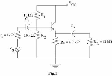
![]() , hfc
=76
, hfc
=76![]() , hib =
27.60
, hib =
27.60![]() . (i) Calculate the circuit input and output impedance with RL
not connected.(ii) calculate Zi
and AV with RL connected.
. (i) Calculate the circuit input and output impedance with RL
not connected.(ii) calculate Zi
and AV with RL connected.
(7)
Q.4 a. With
neat diagram explain the working of depletion-enhancement MOSFET (10)
b. Compare the performance of
the three basic JFET circuits in term of the difference between ID(max)
and ID(min) (6)
Q.5 a. With a neat diagram explain the working of a transformer
coupled class A power amplifier and obtain an expression for theoretical
maximum power conversion efficiency. (10)
b. Explain the construction and
operation of light emitting diode (LED). (6)
Q.6 a. Draw the circuit of op amp
differential amplifier and explain. Obtain expression for output voltage. (8)
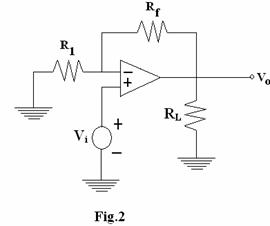
b. For the Fig.2 shown below let R1 =5
k![]() ,0 Rf = 20 k
,0 Rf = 20 k![]() and
and ![]() A load resistor of 5 k
A load resistor of 5 k![]() is connected at the output. Calculate (i)
is connected at the output. Calculate (i) ![]() (ii) ACL (iii) the
load current iL. (4)
(ii) ACL (iii) the
load current iL. (4)
c. Calculate the
maximum frequency of undistorted sine wave that can be obtained at the output
of an op amp which has a slew rate of 1 V/![]() sec when input is a sine wave with a peak of 10 V. (4)
sec when input is a sine wave with a peak of 10 V. (4)
Q.7 a. Draw the circuit of a full wave precision
rectifier, explain with suitable waveforms. (8)
b. Draw the circuit of an
instrumentation amplifier using three Op-amps.
Derive expression for output voltage. (8)
Q.8 a. Draw the circuit of a
monostable multivibrator using 555 timer, and derive the expression for pulse
period. (9)
b. Draw the circuit of an
inverting Schmitt trigger and calculate VUT and VLT
if R1 = 50 k![]() , R2 = 1 k
, R2 = 1 k![]() , Vref =
0 and Vi = 1 Volt peak to peak sine wave and saturation voltages
, Vref =
0 and Vi = 1 Volt peak to peak sine wave and saturation voltages ![]() 14 V. Draw input,
output waveform and draw the transfer characteristics. (7)
14 V. Draw input,
output waveform and draw the transfer characteristics. (7)
Q.9 a. With a diagram explain the working of successive
approximation ADC. (10)
b. Design
a voltage regulator using 723 to get an output voltage of 3 V. Draw the
circuit. (6)