DipIETE
– ET (OLD SCHEME)
 Code: DE06 Subject:
BASIC ELECTRONICS
Code: DE06 Subject:
BASIC ELECTRONICS
Time: 3 Hours
Max. Marks: 100
NOTE: There are 9 Questions in all.
· Question 1 is
compulsory and carries 20 marks. Answer to Q.1 must be written in the space
provided for it in the answer book supplied and nowhere else.
· Out of the
remaining EIGHT Questions, answer any FIVE Questions. Each question carries 16
marks.
· Any required data
not explicitly given, may be suitably assumed and stated.
Q.1 Choose the correct or the best alternative in the following: (2![]() 10)
10)
a.
Respective resistance values and wattage ratings of wire wound
resistors are __________.
(A)
from ![]() to
to ![]() and 400 W
and 400 W
(B) from ![]() to
to ![]() and
200 W
and
200 W
(C)
from ![]() to
to ![]() and 300 W
and 300 W
(D) from ![]() to
to ![]() and
200 W
and
200 W
b. In a semiconductor, the movement of holes is due
to ___________.
(A)
movement of electrons in conduction band
(B)
movement of holes in conduction band
(C) movement of holes in valence band
(D) movement of electrons in valence band
c. In a P-N junction, the barrier Potential offers
opposition to only _________.
(A)
holes in P-region
(B)
free electrons in N-region
(C) majority carriers in both regions
(D) minority carriers in both regions
d. If
the output voltage of a bridge rectifier is 100 V, the Peak Inverse Voltage
(PIV) of diode will be ________.
(A) ![]() (B)
(B) ![]()
(C) ![]() (D)
(D)
![]()
e Which
of the following diodes show the negative resistance region?
(A)
P-N junction (B) Zener
(C) Tunnel (D) Schottky
f. In
an N-P-N transistor collector current is ___________.
(A)
more than emitter current
(B)
less than emitter current, approximately equal to 0.95 time of
emitter current
(C) exactly equal to emitter current
(D) approximately equal to half of the emitter
current
g. In a JFET, drain current will be maximum when
gate-source voltage is ______.
(A)
equal to ![]() (B) positive
(B) positive
(C) negative (D) zero
h. The
triac is equivalent to ___________.
(A)
two SCRs connected in Parallel
(B)
two SCRs connected in antiparallel
(C) one SCR, one diode connected in Parallel
(D) one
diode, one SCR connected in antiparallel
i. An
inverting op-amp has ![]() and
and![]() . Its scale factor is
________.
. Its scale factor is
________.
(A) 1000 (B) –1000
(C) ![]() (D)
(D) ![]()
j.
Ultraviolet radiation is used in IC fabrication process for _______.
(A)
diffussion (B) masking
(C) isolation (D)
metalization
Answer any FIVE
Questions out of EIGHT Questions.
Each question
carries 16 marks.
Q.2 a. What is a passive circuit element? Name the most commonly used passive circuit
elements. Briefly explain the following:
(i)
Paper capacitors.
(ii) Mica capacitors. (9)
b. Differentiate
between a current source and a voltage source. Give their graphical
representations. Convert 4A source with
its parallel resistance of ![]() into its equivalent
voltage source. (7)
into its equivalent
voltage source. (7)
Q.3 a. What is a semiconductor? Explain the formation of N-type material from
intrinsic semi-conductor by proper impurity doping. (10)
b. A
specimen of germanium at ![]() for which the density
of carriers is
for which the density
of carriers is![]() , is doped with impurity atoms such that there is one
impurity atom for
, is doped with impurity atoms such that there is one
impurity atom for ![]() germanium atoms. All the impurity atoms may be assumed
ionized. The receptivity of doped material is
germanium atoms. All the impurity atoms may be assumed
ionized. The receptivity of doped material is ![]() .
.
Carrier
mobility for germanium at ![]() is 3,600. For the doped material, find the electron and
whole densities. Given that the electron charge (e) is
is 3,600. For the doped material, find the electron and
whole densities. Given that the electron charge (e) is![]() . (6)
. (6)
Q.4 a. Discuss how a depletion layer is formed in a
P-N diode and how does it vary with biasing?
Draw the V-I characteristics of P-N junction diode. (10)
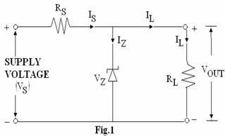
b. Determine
the current flowing through the Zener diode for the circuit as shown in Fig.1, if
![]() , input voltage is 50 V,
, input voltage is 50 V, ![]() and output voltage is
30 V. (6)
and output voltage is
30 V. (6)
Q.5 a. What is a voltage multiplier? What are its applications? Draw the circuit diagram of half-wave voltage
doubler and explain its operation with input and output waveforms. (10)
b. A single-phase Full-Wave Rectifier uses two
diodes, has the internal resistance of each being![]() . The transformer rms secondary voltage from centre-tap to
each end of secondary is 50 V and load resistance is
. The transformer rms secondary voltage from centre-tap to
each end of secondary is 50 V and load resistance is![]() . Find
. Find
(i) The mean load Current![]() .
.
(ii) rms load Current ![]() and
and
(iii)
Output efficiency![]() . (6)
. (6)
Q.6 a. Sketch
a family of CB output characteristics for an NPN transistor and indicate the
Active, Cut-off, Saturation and Break-down regions. Explain the shapes of the curves
qualitatively. (10)
b. The
reverse leakage current of the transistor when connected in CB configuration is
![]() and it is
and it is ![]() when the same transistor is connected in CE
configuration. Assume that the base
current,
when the same transistor is connected in CE
configuration. Assume that the base
current, ![]() is 30 mA and find
is 30 mA and find
(i) Collector Current![]() .
.
(ii) Common Base ![]() and
and
(iii)
Common Emitter ![]() of the transistor. (6)
of the transistor. (6)
Q.7 a. What is the significant difference between
the construction of an Enhancement type MOSFET and a Depletion type
MOSFET? Explain the operation of an
N-channel Enhancement MOSFET. (10)
b. For an N-channel JFET, if ![]() and
and![]() . Find the values
of
. Find the values
of
(i) Drain Current![]() .
.
(ii)
Transconductance for ![]()
![]() and
and
(iii) Transconductance ![]() . (6)
. (6)
Q.8 a. What
are the various types of electron emissions?
Explain in detail, the photoelectric emission. (6)
b. With neat diagrams, explain
the construction, operation and characteristics of SCR. Mention its applications. (10)
Q. 9. a. Draw
the circuit diagram of differentiator using op-amp and derive an expression for
its output voltage. (6)
b. Determine
the output voltage for the op-amp circuit as shown in Fig.2, if ![]()
![]() and
and ![]() (4)
(4)
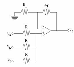
Fig.2
c. Write
a short note on IC resistors. (6)