![]()
AMIETE
– ET/CS/IT (NEW SCHEME) - Code: AE54/AC54/AT54
Subject: LINEAR ICs & DIGITAL ELECTRONICS
 Time: 3 Hours
Max. Marks: 100
Time: 3 Hours
Max. Marks: 100
NOTE: There are 9 Questions in all.
· Question 1 is compulsory and
carries 20 marks. Answer to Q. 1 must be written in the space provided for it
in the answer book supplied and nowhere else.
· Out of the remaining EIGHT
Questions answer any FIVE Questions, selecting at least TWO questions from each
part, each question carries 16 marks.
· Any required data not
explicitly given, may be suitably assumed and stated.
Q.1 Choose
the correct or the best alternative in the following: (2![]() 10)
10)
a. For an Op-amp, the slew rate equation is given
by SR = __________.
(A) ![]() (B)
(B) ![]()
(C) ![]() (D) None of
the above
(D) None of
the above
b. For
the Op-amp Wein-bridge oscillator shown in Fig.1, the gain condition to be
satisfied for oscillations is _________.
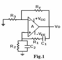
(A) RF ![]() 2R3
2R3
(B) RF ![]() 20R3
20R3
(C) RF ![]() 2R3
2R3
(D) RF ![]() 20R3
20R3
c. The
pulse width of a monostable multivibrator using 555 timers is given by _______.
(A) TP
= 6.93 RC (B) TP
= 0.693 RC
(C) TP
= 1.121 RC (D) TP
= 1.1 RC
d. For a 10 bit
ladder type DAC, the variation in resistance values from LSB to MSB ranges from
________.
(A) R to 10 R (B) R to 1024
R
(C) R to 512 R (D) R to 2 R
![]()
e. For an 8-bit
ADC with Vref = 5 Volt, the value of resolution is _________.
(A) 19.6 mV (B) Zero
(C) 255 mV (D) 5 V
f. For the Op-amp Schmitt Trigger shown in Fig.2, the LTP and UTP
values are given by __________.
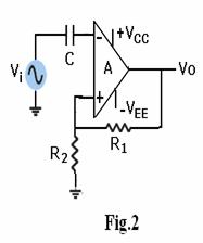
(A) ![]()
(B) ![]()
(C) ![]() and
and ![]()
(D) ![]() and UTP = 0
and UTP = 0
g. An Op-amp buffer with a peak input amplitude of
3.183V and slew rate of 2V/ μS can produce an undistorted output signal if
the input frequency is a maximum of __________.
(A) 500 kHz (B) 100 kHz
(C) 50 kHz (D) 1500 kHz
h. The combination
of an ALU, a control unit and a set of registers on a
single IC chip is called as a ___________.
(A) Microcontroller (B)
Assembler
(C) Compiler
(D) Microprocessor
i. Race around is a problem encountered in _____
F/F and is eliminated in ________ F/F.
(A) a SR, a clocked SR (B) a clocked SR, a JK
(C) a JK, a
MSJK (D) None
j. A pair, a
quad, an octet are the terms associated with __________.
(A) a JK F/F (B) Karnaugh
Map
(C) Synchronous
counter (D) Asynchronous
counter
![]()
PART (A)
Answer At least TWO questions.
Each question carries 16 marks.
Q.2 a. Perform the dc analysis for a differential
amplifier circuit (![]() stage
of an Op-amp) and obtain the equations for operating point. (6)
stage
of an Op-amp) and obtain the equations for operating point. (6)
b. What are the
characteristics of an ideal Op-amp? (6)
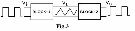
c. For the block diagram shown in
Fig.3, draw different circuits required. (4)
Q.3 a. What is the importance of Slew rate for an Op-amp? Derive an
expression for Slew rate of an Op-amp. (8)
b. A square wave with a negligible rise time and a peak-to-peak
amplitude of 500mV is to be amplified to a peak-to-peak of 3V with a rise time
of 4 μs or less using an Op-amp;
(i) Can A-741 be used? (ii)
Can LM-318 be used?
(Hint: SR for μA-741=
0.5V/μS and LM-318 = 50V/μS). (4)
c. Draw the block diagram of an Op-amp and mention the role of
last stage. (4)
Q.4 a. With a neat diagram explain the working
of a triangular waveform generator. (9)
b. Design an
astable multivibrator using IC-555 for the following specifications; output frequency
of 5 kHz, a duty cycle of 0.65 and output amplitude of 12V. (7)
Q.5 a. Draw the circuit of an Op-amp series voltage
regulator and explain its working. (8)
b. With a neat
diagram explain the working of a Dual slope ADC. (8)
![]()
PART (B)
Answer At least TWO questions.
Each question carries 16 marks.
Q.6 a. Prove
the universality of NAND and NOR gates. (8)
b. Simplify the following switching function
using K-map and implement the result using only NAND gates;
F(A, B,C,D) = åm(0,3,5,6,9) + åd(10,11,12,13,14,15). (8)
Q.7 a. Convert the following POS function in to an
SOP function;
F (A, B, C, D) = A(C+D)'(B'+D') + C (B+C'+A'D). (7)
b. With a neat
diagram explain the working of a JK flip-flop, include preset and clear inputs.
Also justify that Preset and clear inputs are asynchronous input. (9)
Q.8 a. Draw
and briefly explain the working of a Full-adder circuit. (4)
b. Design and
implement a 2-bit magnitude comparator. (8)
c. Realize a 4:1 multiplexer using NAND gates. (4)
Q.9 a. What is modulus of a counter? Explain the
working of a Mod-8 up/down counter. (8)
b. Explain the
serial input and serial output operations of a 4-bit Shift register.
Include the provision for non-destructive readout
operation. (8)