AMIETE
– ET/CS/IT (NEW SCHEME) – Code: AE53/AC53/AT53
Subject: ELECTRONIC DEVICES & CIRCUITS
 Time: 3 Hours
Max. Marks: 100
Time: 3 Hours
Max. Marks: 100
NOTE: There are 9 Questions in all.
· Question 1 is compulsory and
carries 20 marks. Answer to Q.1 must be written in the space provided for it in
the answer book supplied and nowhere else.
· Out of the remaining EIGHT
Questions answer any FIVE Questions. Each question carries 16 marks.
· Any required data not
explicitly given, may be suitably assumed and stated.
Q.1 Choose
the correct or the best alternative in the following: (2![]() 10)
10)
a. Percentage
regulation of a voltage regulator is given by __________.
(A) ![]() (B)
(B) ![]()
(C) ![]() (D)
(D) ![]()
b. For a SCR, the
two transistor analogy holds good when the SCR is in _________
(A) Forward
Blocking State (B) Conduction
state
(C) Both (A) & (B) (D) None
c. The maximum
conversion efficiency of a transfer coupled Class-A amplifier is
(A) 75 % (B) 50 %
(C) 95 % (D) 78.5 %
d. Node
defines
(A) the point
where two or more elements meet.
(B) is a loop that does
not contain any other loop within it.
(C) a
traversal through elements.
(D) None
of the above
e. Common base
forward short-circuit current gain given by
(A) ![]() (B)
(B) ![]()
(C) ![]() (D)
(D) ![]()
f. The
disadvantage of complimentary symmetry circuit is
(A) it requires one power supply.
(B) it requires two power supply.
(C) it requires more than one power
supply.
(D) Both
(B) and (C).
g. The most
popularly used transistor biasing circuit is
(A) Fixed
Bias (B) Feedback
Bias
(C) Potential
Divider Bias (D) None
h. Feedback in an amplifier increases the input
impedance from ![]() to
to ![]() because of
because of
(A) positive
feedback (B) shunt-current
negative feedback
(C) series-current
negative feedback (D) shunt-voltage
negative feedback
i. SSI technology includes ______number of gates
on chip.
(A) Less than
10 (B) 10 to 100
(C) 100 to
500 (D) More than
100
j. In a RC-phase shift oscillator having three
stages, which have equivalent resistors and capacitors, in order to satisfy
Barkhausen criteria, should have a minimum gain of
(A) 6 (B) 29
(C) 31 (D) 49
Answer any FIVE Questions out
of EIGHT Questions.
Each question carries 16
marks.
Q.2 a. State and explain reciprocity theorem with
example. (6)
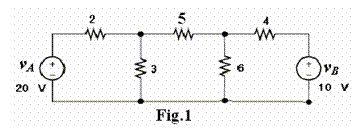
b. Using
Thevenin’s theorem find the current flowing through 4 ![]() resistor in the network of Fig.1; (All
resistances in
resistor in the network of Fig.1; (All
resistances in ![]() ) (10)
) (10)
Q.3 a. Explain
Zener diode as voltage regulator. (8)
b. For the diode circuit of Fig.2, find the diode current, the
diode parameters are
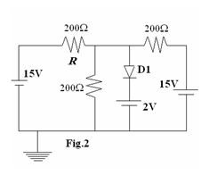
![]() ,
, ![]()
![]()
![]() . (8)
. (8)
Q.4 a. Draw
and explain Common Emitter Configuration. (6)
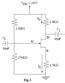
b. For
the JFET circuit shown in Fig.3 find IDQ, VGSQ and VDSQ if VP = -4V, IDSS=
8mA and VDD = 16V. (10)
Q.5 a. Derive an expression for Stability factor ![]() of
a biasing circuit. (8)
of
a biasing circuit. (8)
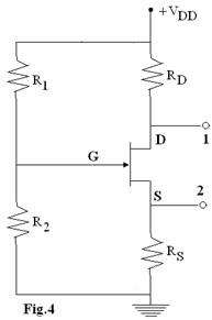
b. Consider the
JFET circuit of Fig.4
(i)
Determine the resistance seen from terminal 2 and ground at low
frequencies.
(ii)
Evaluate the resistance in part (i) for ![]()
![]()
![]() and
and ![]() .
(8)
.
(8)
Q.6 a. Explain
various distortions occurred in small signal amplifiers. (8)
b. Draw and explain the tuned amplifier and determine
its quality factor. (8)
Q.7 a. Draw the transformer coupled power amplifier
and calculates its maximum possible efficiency. (8)
b. Calculate the
maximum conversion efficiency of complimentary symmetry circuit amplifier. (8)
Q.8 a. Explain
Phase Shift Oscillator. (8)
b. Write a short
note on Crystal Oscillator. (8)
Q.9 a. What is an epitaxial layer and how is it
grown? Explain the necessity of this
layer as a first step on the substrate. (8)
b. Explain the
electron beam lithography. What
advantages does it have over photolithographic process? (8)