AMIETE
– ET/CS/IT (NEW SCHEME) – Code: AE53/AC53/AT53
Subject: ELECTRONIC DEVICES AND CIRCUITS
 Time: 3 Hours
Max. Marks: 100
Time: 3 Hours
Max. Marks: 100
NOTE: There are 9 Questions in all.
· Question 1 is compulsory and
carries 20 marks. Answer to Q.1 must be written in the space provided for it in
the answer book supplied and nowhere else.
· Out of the remaining EIGHT
Questions, answer any FIVE Questions. Each question carries 16 marks.
· Any required data not
explicitly given, may be suitably assumed and stated.
Q.1 Choose
the correct or the best alternative in the following: (2![]() 10)
10)
a. The Network Theorem used to find the
equivalent circuit across an open circuited terminal is __________.
(A) Thevenin’s
Theorem (B) Superposition
Theorem
(C) Reciprocity
Theorem (D) None of
the above
b. The change in output voltage from no-load to
full-load condition is called _________.
(A) Rectification (B) Regulation
(C) Efficiency (D) Filtering
c. The Zener diode
in a Zener voltage regulator is working in its _______ region.
(A) forward
biased (B) reverse
biased
(C) zero
biased (D) Both (A) and (B)
d. A transistor
switch will be biased to work in its ________ region of operation.
(A) cut-off
and Saturation (B) cut-off
and Active
(C) active
and Saturation (D) None of
the above
e. For a SCR, in
the forward blocking state the SCR is _________.
(A) Forward
biased and very little current flows
(B) Forward
biased and little current flows
(C) Reverse
biased and very little current flows
(D) None
f. The most
popularly used transistor biasing circuit is
(A) Fixed
Bias (B) Feedback
Bias
(C) Potential
Divider Bias (D) None
g. The _______configuration of a transistor offers a
phase reversal between I/P and O/P.
(A) common emitter (B) common base
(C) common collector (D) None
h. The maximum
conversion efficiency of a transformer coupled Class-A amplifier is
(A) 75 % (B) 50 %
(C) 95 % (D) 78.5 %
i. An UJT can be used in the construction of
(A) an oscillator (B) an
amplifier
(C) Both (A) and (B) (D) a rectifier
j. MSI technology
includes ______number of gates on the chip.
(A) less than
10 (B) 10 to 100
(C) more than
10000 (D)100 to10000
Answer any FIVE Questions out
of EIGHT Questions.
Each question carries 16
marks.
Q.2 a. List all the conditions in a series RLC
circuit under resonance. Obtain an expression for resonance frequency of a
series RLC circuit. (10)
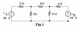
b. For the
network shown in Fig.1 apply Thevenin’s theorem and find the voltage across
5Ω resistor. (6)
Q.3 a. Compare
performance of a half wave rectifier, a centre tapped full wave rectifier and a
bridge type full wave rectifier. (8)
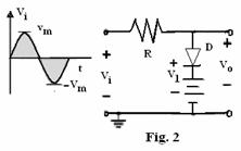
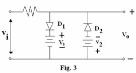
b. Input to the clipping circuits shown in Fig.2 and Fig.3 is a sine wave of 10V peak; draw
the output wave forms assuming ideal diodes and |v1| =4V & |v2|
= 2V. (8)
Q.4 a. Draw
and explain the I/P and O/P characteristics of a transistor CE configurations. (8)
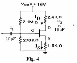
b. For the JFET
circuit shown in Fig. 4 find ID and VDS if VP
= – 4V and VDD = 16 V. (8)
Q.5 a. Explain how to measure the performance of a
biasing network? Derive an expression for Stability factor ‘S’. (8)
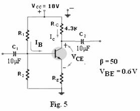
b. For the
potential divider bias circuit shown in Fig.5 find the values of all resistors
such that operating point Q = (1.5 mA, 10 V) and stability factor ![]() . (8)
. (8)
Q.6 a. Draw a two stage RC coupled amplifier circuit
diagram, explain the importance of each biasing component and draw its
frequency response. (9)
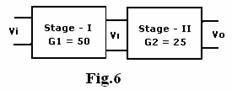
b. Why amplifiers cascading is required? A
Multistage Cascaded amplifier in Fig.6 has 2 stages with A1 = 50 and
A2 = 25. If Vi = 5mV,
find V1, VO and the overall dB gain of the cascaded
system. (7)
Q.7 a. What
do you mean by the following terms? Use suitable diagrams to explain.
(i)
Class-A Power Amplifier (ii) Class-B Power Amplifier
(iii) Class-C Power Amplifier (iv) Class-AB
Power Amplifier (9)
b. Prove that the
maximum conversion efficiency of a Class-B power amplifier is 78.5%.
(7)
Q.8 a. What
are the effects of Negative feedback on I/P impedance, bandwidth and gain of an
amplifier? Explain. . (6)
b. With a neat
diagram explain the working of a UJT relaxation oscillator and show that TC
= RC ln (1/ (1 – η)). (10)
Q.9 a. Briefly explain the steps involved in IC
fabrication. (8)
b. Calculate the
chip area needed for a 250 pF MOS capacitor given the thickness of SiO2
layer is 500 Å units and the relative dielectric constant (εr)
is 3.5. It is required to reduce the chip area by 20%, what should be the new
thickness of SiO2 layer? (8)