AMIETE – ET (OLD SCHEME)
Code: AE09 Subject: ANALOG & DIGITAL ELECTRONICS
 Time: 3 Hours
Max. Marks: 100
NOTE: There are 9 Questions in all.
· Question 1 is compulsory and
carries 20 marks. Answer to Q.1 must be written in the space provided for it in
the answer book supplied and nowhere else.
· Out of the remaining EIGHT
Questions answer any FIVE Questions. Each question carries 16 marks.
· Any required data not
explicitly given, may be suitably assumed and stated.
Q.1 Choose
the correct or the best alternative in the following: (2![]() 10)
10)
a. Relation between unity gain
frequency (![]() ) and break frequency (
) and break frequency (![]() ) is
) is
(A) ![]() . (B)
. (B)
![]() .
.
(C) ![]() (D)
(D)
![]()
b. –3 dB frequency is at which power
(A) Increased to half of the maximum
frequency.
(B) Reduced to half of the maximum
frequency.
(C) Increased to half of the minimum frequency.
(D) Reduced to half of the minimum frequency.
c. Maximum resistor ratio required by 12 bit D/A converter using binary weighted ladder is
(A) 1024 (B) 2048
(C) 512 (D)
1064
d. Two 16:1 and one 2:1 multiplexers can be connected to form a
(A)
16:1
Mux (B) 32:1 Mux
(C) 64:1 Mux (D) 8:1
Mux
e. TTL uses
(A) Multiemitter transistor
(B) Multibase transistor
(C) Multicollector transistor
(D) Multiemitter & multicollector transistor
f. A device which converts BCD to seven segment is called
(A) Encoder (B) Decoder
(C) Multiplexer (D) None of these
g. A + (B.C) =
(A) B.A + C (B)
A.B + A.C
(C) A (D)
(A+B).(A+C)
h. Which memory is available in all technology?
(A) PROM (B)
EEPROM
(C) ROM (D) EPROM
i. A counter has N flip flops. The total numbers of states are
(A)
N (B)
2N
(C) ![]() (D)
4N
(D)
4N
j. As compare to TTL, ECL has
(A) Lower power dissipation. (B) Higher propagation
delay.
(C)
Lower
propagation delay. (D) Higher noise margin.
Answer any FIVE Questions out of EIGHT
Questions.
Each question carries 16 marks.
Q.2 a. What is a magnitude comparator? Draw a logic
circuit for 1 bit comparator. (8)
b. Draw a sample and
hold circuit and explain its operation. (8)
Q.3 a. A low pass Butterworth filter is to be
designed to have a 3 dB bandwidth of 200 Hz and the attenuation of 60 dB at 400
Hz. Find the order of the filter. (8)
b. Explain how an FET can be used as a switch. (8)
Q.4
a. Calculate ![]() for the given circuit in Fig.1 for
for the given circuit in Fig.1 for ![]() . (6)
. (6)
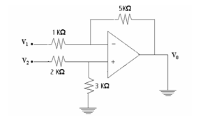
Fig. 1
b. Draw the basic TTL logic NAND gate and explain it. (10)
Q.5 a. Discuss
the working of CMOS as two input NOR gate. (8)
b. Explain the terms:- (i) Input offset voltage (ii) Input bias current
(iii)
Input offset current (iv) Slew rate. (2![]() 4)
4)
Q.6 a. Explain the operation of logarithmic
amplifier using one op-amp. (6)
b. Design a 5 Mod
synchronous binary counter using D flip flop.
(10)
Q.7 a. Explain the working of Decimal to BCD
encoder. (8)
b.
Calculate: (i) the current through the collector resistor Rc and
(ii) the
collector current in each transistor. Assume VBE =0.7 V and β =100. (8)
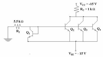
Fig. 2
Q.8 a. Draw
a regenerative comparator and explain its operation.
(8)
b. What is a Schottky
diode? Comment on the storage time of Schottky diode. (8)
Q.9 Write short notes on any TWO of the following: -
(i)
Charge coupled device.
(ii)
Seven segment display system.
(iii)
Shift registers.
(iv)
Parity check generator. (8![]() 2)
2)