AMIETE – ET (OLD SCHEME)
 Code: AE05 Subject:
BASIC ELECTRONICS
Code: AE05 Subject:
BASIC ELECTRONICS
Time: 3 Hours Max. Marks: 100
NOTE: There are 9 Questions in all.
· Question 1 is compulsory and
carries 20 marks. Answer to Q.1 must be written in the space provided for it in
the answer book supplied and nowhere else.
· Out of the remaining EIGHT
Questions answer any FIVE Questions. Each question carries 16 marks.
· Any required data not explicitly
given, may be suitably assumed and stated.
Q.1 Choose
the correct or the best alternative in the following: (2![]() 10)
10)
a. In a bipolar junction transistor,
a change of 160 mV in ![]() causes a change of
causes a change of ![]() in its base current. The
dynamic input resistance of the transistor in CE configuration is
in its base current. The
dynamic input resistance of the transistor in CE configuration is
(A) ![]() (B)
(B) ![]()
(C) ![]() (D)
(D) ![]()
b. Frequency response of a small signal amplifier is a graph showing the variation of
(A)
Frequency
of the signal vs transistor ![]()
(B)
Resonant
frequency vs amplifier gain
(C) Frequency vs amplifier efficiency
(D) Amplifier gain vs frequency of input signal.
c. The maximum collector circuit efficiency of an ideal transformer-coupled class A amplifier is
(A) 25% (B)
50%
(C) 78.5% (D) 100%
d. The voltage gain of an amplifier is 150. Negative
feedback with ![]() is applied to the amplifier. The gain of the amplifier with feedback is
is applied to the amplifier. The gain of the amplifier with feedback is
(A)
15 (B)
50
(C) 99.94 (D)
100.6
e. For generating sinewave of 2 kHz, the most suitable oscillator circuit is
(A)
(C) Clapp oscillator (D)
Hartley oscillator
f. The differential mode gain of a differential amplifier is 500 and its common-mode gain is 0.05. The CMRR of the amplifier is
(A) 20 dB (B)
40 dB
(C) 80 dB (D) 100 dB
g. To obtain a rectangular voltage waveform from a sinusoidal voltage wave, the most suitable circuit is a
(A) Clipping circuit (B)
Clamping circuit
(C) Monostable multivibrator (D) Schmitt Trigger
h. In a good quality regulated power supply, the
value of the parameter, ![]() (output resistance),
should be
(output resistance),
should be
(A) as small as possible (B) as large as possible
(C) equal to load resistance (D) none of these
i. When the literals ![]() and
and ![]() each are fed to the two inputs of NOR gate, the output of the
gate is equal to
each are fed to the two inputs of NOR gate, the output of the
gate is equal to
(A) X+Y (B) ![]()
(C) ![]() (D)
(D)
![]()
j. In a digital system having 4 inputs, the total number of input combinations are
(A) 4 (B) 8
(C) 16 (D)
32
Answer any FIVE Questions out
of EIGHT Questions.
Each question carries 16
marks.
Q.2 a. What is ‘Hall effect’? Explain how it may be used to measure
mobility of charge carriers in semiconductors.
(10)
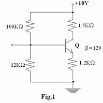
b. Determine the Q-point ![]() in the transistor
circuit shown in Fig.1. The
in the transistor
circuit shown in Fig.1. The ![]() of the transistor is
120. (6)
of the transistor is
120. (6)
Q.3 a. Draw
the circuit diagram of a single stage, common-emitter BJT RC- coupled amplifier and explain the role of
each component used in the circuit. Show
the h-parameter equivalent circuit of the amplifier applicable for midfrequency
range, and thereby find an expression for voltage gain in midfrequency region. (9)
b. Write the circuit of Darlington Amplifier. Analyse the circuit to obtain an expression for its overall current gain. (7)
Q.4 a. Define the various classes of amplifiers based on biasing (location of Q point) considerations. Also state the advantages and disadvantages of class B amplifier in comparison with class A operation. (4+3)
b. Compute
the input impedance, output impedance and voltage gain of the FET circuit shown
in Fig.2. For the FET, ![]() (4)
(4)
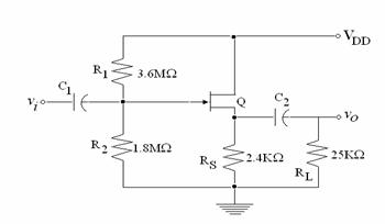
Fig.2
c.
A sinusoidal signal ![]() is fed to a power
amplifier. The resulting output current is of the from
is fed to a power
amplifier. The resulting output current is of the from
![]() . Find the percentage harmonic distortion due to the second,
third and the fourth harmonics. Also
calculate the overall distortion factor due to these harmonics. (5)
. Find the percentage harmonic distortion due to the second,
third and the fourth harmonics. Also
calculate the overall distortion factor due to these harmonics. (5)
Q.5 a. An amplifier with intrinsic gain A, is
modified with negative feedback having feedback factor![]() . Obtain an expression
for gain with the feedback. Also show
how gain stabilization is improved with negative feedback. (5)
. Obtain an expression
for gain with the feedback. Also show
how gain stabilization is improved with negative feedback. (5)
b. An amplifier having intrinsic gain of 600 is
applied with negative feedback of ![]() . Compute the change
in the overall gain of the feedback amplifier if the intrinsic gain of the
amplifier is reduced by 20%. (3)
. Compute the change
in the overall gain of the feedback amplifier if the intrinsic gain of the
amplifier is reduced by 20%. (3)
c. What are the advantages of using a crystal in
an oscillator? Draw the equivalent
electric circuit of a crystal for an oscillator. Calculate the series and parallel resonant
frequencies of a crystal having ![]() ,
,![]() ,
, ![]() ,
, ![]() . Also find the Q of the crystal. (8)
. Also find the Q of the crystal. (8)
Q.6 a. Show the block schematic of a typical op-amp and describe briefly the function of each block. (8)
b. Name the function of the circuit shown in Fig.3
and derive an expression for
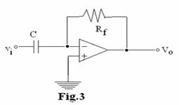
![]() . (4)
. (4)
c. In the op-amp circuit
shown in Fig.4, show that the current ![]() is independent of
is independent of![]() , hence, identify the function of the circuit. (4)
, hence, identify the function of the circuit. (4)
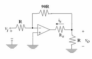
Fig.4
Q.7 a. Draw the circuit of a monostable
multivibrator using an op-amp and describe its operation with the help of
waveforms of voltages at relevant nodes. (10)
b. Show how a ramp generator can be constructed
using an op-amp and transistor. Describe
its operation. (6)
Q.8 a. Why filters are necessary along with basic
rectifiers to construct a power supply? Draw neat sketches to show the
following waveforms. No explanation
required. (7)
(i) output voltage of a full-wave rectifier with
L filter.
(ii) output voltage of a half-wave rectifier with
C filter.
(iii) output voltage of a
full-wave rectifier with C filter.
Mark all the quantities
clearly.
b. Draw the
circuit of a fold back current limiter which can be used with a series
regulator, and explain its operation. (9)
Q.9 a. Using the three Boolean Algebra variables A,
B and C write simple expressions to illustrate the following theorems
(laws). Write also the expression for
the dual in each case. (4)
(i) Commutative law; (ii) Associative law;
(iii)
Distributive law; (iv)
De Morgan’s law.
b. Simplify the Boolean
function given below in
(i) SOP form and
(ii) POS form. Use Karnaugh maps. Draw the logic diagram for both the results
using suitable gates. (8)
![]()
c. Construct
a 4-bit ring counter using D flip-flops and explain its operation by writing
timing diagrams. (4)