Code: AE-05
Subject: BASIC ELECTRONICS
PART - I, VOL – I
TYPICAL QUESTIONS & ANSWERS
OBJECTIVE TYPE QUESTIONS
Each Question carries 2 marks.
Choose correct or the best alternative
in the following:
Q.1 When the temperature of a duped
semiconductor is increased, its conductivity
(A) decreases.
(B) increases.
(C) does not change.
(D) increases
or decreases depending on whether it is p- or n-type.
Ans: B
Q.2 The main characteristics of a
Darlington Amplifier are
(A)
High input impedance, high output impedance
and high current gain.
(B)
Low input impedance, low output impedance
and low voltage gain.
(C)
High input impedance, low output impedance
and high current gain.
(D)
Low input impedance, low output impedance
and high current gain.
Ans:
C
Q.3 The transconductance, gm, of a JFET is computed at
constant VDS, by the following:
(A)
 (B)
(B)

(C)
 (D)
(D)

Ans:
A
Code: AE-05 BASIC
ELECTRONICS

Q.4 The feedback factor β at the frequency of oscillation of a Wien bridge oscillator is
(A)
3 (B) 
(C)
 (D)
(D)

Ans:
B
Q.5 In an amplifier with negative feedback, the bandwidth is
(A)
increased by a factor of β
(B)
decreased by a factor of β
(C)
increased by a factor of (1+Aβ)
(D)
not affected at all by the feedback
where A = gain of the basic amplifier and β = feedback factor
Ans:
C
Q.6 The ‘slew rate’ of an operational amplifier indicates
(A)
how fast its output current can change
(B)
how fast its output impedance can change
(C)
how fast its output power can change
(D)
how fast its output voltage can change
when a step input signal is given.
Ans:
D
Q.7 In a clamping circuit, the peak-to peak voltage of the waveform
being clamped is
(A)
affected by the clamping
(B)
not affected by the clamping
(C)
determined by the
clamping voltage value
(D)
determined by the ratio of rms voltage of
the waveform and the clamping voltage
Ans:
B
Q.8 Regulation of a.d.c. power supply is given by
(A)
product of no-load output voltage and
full-load current
(B)
ratio of full-load output voltage and
full-load current
(C)
change in output voltage from no-load to
full-load
(D)
change in output impedance from no-load to
full-load
Ans:
D
Code: AE-05 BASIC
ELECTRONICS
Q.9 A ‘literal’ in Boolean Algebra
means
(A)
a variable inn its uncomplemented form only
(B)
a variable ORed with its complement
(C)
a variable in its complemented form only
(D)
a variable in its complemented or
uncomplemented form
Ans:
D
Q.10 In an unclocked R-S flip-flop made of NOR gates, the forbidden input
condition is
(A)
R = 0, S = 0 (B) R = 1, S =
0
(C)
R = 0, S = 1 (D) R = 1, S =
1
Ans:
D
Q.11 The current amplification factor in CE configuration is
(A)
α (B)
β + 1
(C)
 (D)
β
(D)
β
Ans:
D
Q.12 A zener diode
(A)
Has a high forward voltage rating.
(B)
Has a sharp breakdown at low reverse
voltage.
(C)
Is useful as an amplifier.
(D)
Has a negative resistance.
Ans:
B
Q.13 N-channel FETs are superior to P-channel FETs, because
(A)
They have a higher input impedance.
(B)
They have high switching time.
(C)
They consume less power.
(D)
Mobility of electrons is greater than that
of holes.
Ans:
Code: AE-05 BASIC
ELECTRONICS
Q.14 The maximum possible collector circuit efficiency of an ideal class
A power amplifier is
(A)
15% (B) 25%
(C)
50% (D) 75%
Ans:
C
Q.15 Negative feedback in an amplifier
(A)
Reduces the voltage gain.
(B)
Increases the voltage gain.
(C)
Does not affect the voltage gain.
(D)
ConvErDs the amplifier into an oscillator.
Ans:
A
Q.16 For generating 1 kHz signal, the most suitable circuit is
(A)
Colpitts oscillator. (B) Hartley
oscillator.
(C)
Tuned collectOr oSc!llator. (D) Wien bridge
oscillator.
Ans:
D
Q.17 Phe output stage of an op-amp is usually a
(A)
Complementary emitter follower.
(B)
Transformer coupled class B amplifier.
(C)
Class A power ampli&ier.
(D) Class B amplifier.
Ans: A
Q.18 When a sinusoidal voltage wave
is fed to a Schmitt trigger, the output will be
(A) triangular wave. (B)
asymmetric square wave.
(C) rectangular wave. (D)
trapezoidal wave.
Ans: B
Code: AE-05 BASIC
ELECTRONICS
Q.19 If the peak value of the input
voltage to a half wave rectifier is 28.28 volts and no filter is use, the
maximum dc voltage across the load will be
(A)  . (B)
15 V.
. (B)
15 V.
(C) 9 V. (D)
14.14 V.
Ans: C
Q.20 The logic gate which detects
equality of two bits is
(A) EX-OR (B)
EX-NOR
(C) NOR (D)
NAND
Ans: B
Q.21 The electron relaxation time of
metal A is  s, that of B is
  s. The
ratio of resistivity of B to resistivity of A will be
s. The
ratio of resistivity of B to resistivity of A will be
(A) 4. (B)
2.0.
(C) 0.5. (D)
0.25.
Ans: B
Q.22 The overall bandwidth of two
identical voltage amplifiers connected in cascade will
(A)
Remain the same as that of a single stage.
(B)
Be worse than that of a single stage.
(C)
Be better than that of a single stage.
(D)
Be better if stage gain is low and worse if
stage gain is high.
Ans:
B
Q.23 Field effect transistor has
(A)
large input impedance. (B) large output
impedance.
(C)
large power gain. (D) large votage
gain.
Ans:
A
Code: AE-05 BASIC
ELECTRONICS
Q.24 Which of the following parameters
is used for distinguishing between a small signal and a large-signal amplifier?
(A) Voltage gain (B)
Frequency response
(C) Harmonic
Distortion (D) Input/output impedances
Ans: D
Q.25 Which of the following
parameters is used for distinguishing between a small signal and a large-signal
amplifier?
(A) Instability (B)
Bandwidth
(C) Overall gain (D)
Distortion
Ans: B
Q.26 If the feedback signal is
returned to the input in series with the applied voltage, the input impedance
______.
(A) decreases (B)
increases
(C) does not change (D)
becomes infinity
Ans: B
Q.27 Most of linear ICs are based on
the two transistor differential amplifier because of its
(A)
input voltage dependent linear transfer
characteristic.
(B)
High voltage gain.
(C)
High input resistance.
(D)
High CMRR
Ans:
D
Q.28 The waveform of the output voltage for the circuit shown in Fig.1
(RC >> 1) is a
(A)
sinusoidal wave (B) square wave
(C)
series of spikes (D) triangular
wave.
Ans:
D
Code: AE-05 BASIC
ELECTRONICS
Q.29 A single phase diode bridge
rectifier supplies a highly inductive load. The load current can be assumed to
be ripple free. The ac supply side current waveform will be
(A) sinusoidal (B)
constant dc.
(C) square (D)
triangular
Ans: C
Q.30 Which of the following Boolean
rules is correct?
(A) A + 0 = 0 (B)
A + 1 = 1
(C)  (D)
(D)

Ans: B
Code: AE-05
BASIC ELECTRONICS
PART – II, VOL – I
NUMERICALS
Q.1 What is ‘doping’ of a
semiconductor? Explain how p- and n-type semiconductors are formed. Also write
their energy band diagrams, clearly showing the different energy levels. (8)
Ans: pp 102 - 104
Q.2 What is Early effect? Explain
how it affects the characteristics of BJT in CB configuration.
(8)
Ans: p. 238 - 39
Q.3 Draw a neat circuit of a
differential amplifier and explain its operation. (8)
Ans: p. 450 - 52
Q.4 In a transformer, give the relationship
between
(i) turns ratio and
its primary and secondary impedances
(ii) turns ratio and primary/secondary voltage.
In a transformer-coupled amplifier, the transformer
used has a turns ratio N1:N2 = 10:1.. If the source impedance is 8 KΩ
what should be the value of load impedance for maximum power transfer to the
load? Also find the load voltage if the source voltage is 10 volts. (6)
Ans: p. 439 – 40
Given:
 ;
;
 -
load side;
-
load side;  - amplifier side or source
side.
- amplifier side or source
side.

Turns ratio and impedances : 
Turns ration and voltages : 
 ; i.e.

Load
voltage = V2 ; 
 .
.
Q.5 Explain the effect of
temperature on a JFET. (8)
Ans: p. 276.
Code: AE-05 BASIC
ELECTRONICS
Q.6 The FET circuit given below in
Fig.1, has R1=3.5MΩ, R2 = 1.5MΩ, RS
= 2KΩ, RL = 20KΩ and gm = 2.5mS. Find its input
impedance, output impedance and voltage gain. (8)
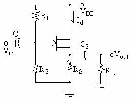
Ans:
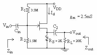
(i) 
(ii) 
(iii)
Voltage gain 
Q.7 State any four advantages of
negative feedback in amplifiers. (5)
Ans: p. 499.
Code: AE-05 BASIC
ELECTRONICS
Q.8 In an amplifier with negative
feedback, the gain of the basic amplifier is 100 and it employs a feedback
factor of 0.02. If the input signal is 40mV, determine
(i) voltage gain with feedback and
(ii) value of output voltage. (3)
Ans:
(i) 
(ii)

Q.9 Describe how oscillations are
developed in a tank circuit. (8)
Ans: p. 655.
Q.10 Draw the circuit of a sample-and-hold circuit using op-amp. Explain
its working with neat timing diagrams. (8)
Ans: p. 834.
Q.11 Define the following terms as applied to characterization of op-amps
(i) CMRR (ii)
slew rate (4)
Ans: p. 800, p. 826.
Q.12 In the circuit shown below in Fig.2, R1=12KΩ, R2
= 5KΩ, R3 = 8KΩ, RF = 12KΩ. The inputs
are: V1 = 9V, V2 = -3V and V3 = -1V. Compute
the output voltage. (4)
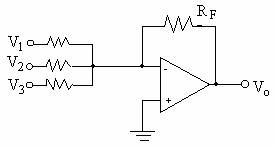
Ans:

= - 12(0.75 – 0.6 – 0.125) = - 0.3 V.
Code: AE-05 BASIC
ELECTRONICS
Q.13 What are the different types of multivibrators? Briefly explain each
type. (7)
Ans: p. 735 – 36.
Q.14 Draw the circuit of an astable multivibrator using 555 timer. Derive
the expression for its frequency of oscillation. (9)
Ans: p. 866 – 67.
Q.15 Draw a neat diagram to show the functional blocks of a complete
reguiated power supply. Explain the role of each block. (9)
Ans: p. 908 – 09.
Q.16 A half-wave rectifier has a load resistance of 3.5 KΩ. If the
diode and secondary of the transformer have a total resistance of 800KΩ
and the ac input voltage has 240 V (peak value), determine:
(i) peak, rms and average values of current
through load
(ii) dc power output
(iii)
ac power input
(iv)
rectification efficiency (7)
Ans:
(i)  = peak
current.
= peak
current.
 = average
current.
= average
current.
 .
.
(ii) DC power output =
 watts.
(iii) ac power input =
 watts.
(iv) Rect. Effect =  .
.
Q.17 Draw the circuit of 4-bit ring counter using suitable flip-flop.
Explain its operation using timing diagrams and truth table. (8)
Ans: p. 1021
Code: AE-05 BASIC
ELECTRONICS
Q.18 Show how a T-flop-flop can be constructed using J-K flip-flop. Write
the truth table of T flip-flop. (2)
Ans: p. 1016
Q.19 Implement AND, OR and NOT gates using (6)
(i) NOR gates only (ii)
NAND gates only
Ans: p. 1001.
Q.20 Explain how Hall effect may be used to measure mobility of charge
carries in semiconductors.
(7)
Ans:
Consider a rectangular bar of semiconductor placed in a transverse
magnetic field B and carrying current I as shown in the figure.
 I
I


 X
X

 B
B


 W Y
W Y
In this situation, a Hall voltage VH will be induced
perpendicular to both I and B directions, i.e. across X and Y in the figure. If
p is charge density due to I, the Hall coefficient is known to be
 is also given by
  …….(1)
If the condition is due to primarily to charges of one sign, the
conductivity σ is related to mobility as σ =
μp …….(2)
RH can be computed by measuring VH
experimentally and using equation(1). Hence, as  and
and  , by which μ
can be determined.
, by which μ
can be determined.
Code: AE-05 BASIC
ELECTRONICS
Q.21 Distinguish between avalanche and zener breakdown in p-n junction
diode. (7)
Ans:
Both avalanche breakdown and zener breakdown occur under
reverse biased condition of p-n junction and the common cause is the electric
field accelerating a carrier which collides with an ion and breaks the covalent
bond releasing one or more extra carriers. In the case of avalanche breakdown,
the carriers are thermally generated ones accelerating under externally applied
large electric field in reverse bias and the process is cumulative giving rise
to more and more pairs of carriers by multiple collision of ions. The result is
destructive.
On the other hand, in a zener diode, the breaking of
ionic bond and generation of extra carriers is by the intense electric field
across a very narrow depletion region at the junction, due mainly to rather
heavy doping of both p and n regions of the diode. The resulting process gives
rise to large reverse current and is reversible. This phenomenon is called
‘Zener breakdown’.
Q.22 A BJT has a base current of 250 μA and emitter current of 15mA
Determine the collector current gain and β. (2)
Ans:
The current relationship in a transistor is given by 
i.e. 
Given:

IE = 15 mA

And
 .
.
Code: AE-05 BASIC
ELECTRONICS
Q.23 Draw the circuit of Darlington amplifier and analyse it to obtain expressions for its current gain and input
impedance. Also mention its merits and application. (10)
Ans: The circuit for Darlington amplifier is shown below

The equivalent circuit for small signal is as shown below

Considering  ……(1)
……(1)
Current Gain:  …..(2)
For transistor Q1, 1/hoel is comparable with becomes
the load impedance for Q1.
Hence without neglecting 1/hoel, the current gain for Q1
is
 ……(3)
……(3)
Code: AE-05 BASIC
ELECTRONICS
If  , equation (3) can be written
as
, equation (3) can be written
as

The overall gain of the amplifier is 
i.e.,  …….(4)
For  , a good approximation would
be ingnored w.r.t Zin2, …..(5)
, a good approximation would
be ingnored w.r.t Zin2, …..(5)

= 
If  then
then

if  , then
The advantage of darlington amplifier is its very high
current gain and very high Zin. It is used to isolate high impedance source
from low impedance load.
Code: AE-05 BASIC
ELECTRONICS
Q.24 In the circuit shown in Fig.1,
[IDSS] = 4mA, Vp = 4V. Find the quiescent values of 1D,
VGS and VDS of the FET. (6)
 Fig.1
Fig.1
Ans: 
The potential divider
bias circuit can be replaced by Thevenin equivalent as shown, where


Applying Kirchoff’s Voltage law to gate–source circuit gives  as there
is no gate current flow.
as there
is no gate current flow.
Hence 
Code: AE-05 BASIC
ELECTRONICS
Given, IDSS = 4 mA and VP = 4 V. substituting
these values in the equation for IP

Forming the quadratic equation in VGS.

Solving, VGS = 3 V(Solution VGS = 4V is not
realistic).
Solving for ID, ID = (1 – ¾) = 0.25 mA
Hence, VDS = 30 – 0.25(18 + 4) = 24.5 Volts.
Q.25 In the transformer coupled
class A amplifier shown in Fig.2 below, the transistor has hFE =
β = 40 and hie = 25Ω. Assume that the transformer is ideal
and that  and
also
and
also  .
Determine values of R1 and R2 to obtain quiescent current
.
Determine values of R1 and R2 to obtain quiescent current
 .
If the collector current swing
.
If the collector current swing  , find the peak values of load
current and load voltage. Transformer turns ratio is primary 1:6 secondary. (10)
, find the peak values of load
current and load voltage. Transformer turns ratio is primary 1:6 secondary. (10)

Ans: The equivalent circuit
replacing R1, R2 as part of thevenin source is shown

Code: AE-05 BASIC
ELECTRONICS
 ……(1)
……(1)  ………(2)
Applying KVL around base-emitter circuit,

i.e.  …….(3)
Any value of RB by which  is
acceptable. Hence, choosing a reasonable value of 2.2K for RB,
is
acceptable. Hence, choosing a reasonable value of 2.2K for RB,  volts.
Use equations (1) and (2) to find R1
and R2
From (1) 
i.e.  ……..(4)
substituting the value of R1 in
equation (2)
 ….(5)
….(5)
simplifying,  ………(6)
From (4) and (6), we get
 ………(7)
using equation (6), 
using equation (7), 
The load Rac at the collector leg of
the transistor is reflected load of RL as per the turns ratio (a) of
the transformer.
i.e. 
As ic swings ± 80 mA either side of ICQ
= 100 mA on the Rac load line, and VCEQ = 12V (DC load
line being almost vertical)

= 12
+ 5.55 = 17.55 Volts.
Code: AE-05 BASIC
ELECTRONICS
Hence, Maximum Load voltage(secondary):

Hence, Maximum Load
current:
 .
.
Q.26 Draw the circuit of common
source amplifier using JFET and show its equivalent circuit. Analyse the
equivalent circuit to find an expression for voltage gain and output
resistance.
(6)
Ans:
The circuit of
n-channel, JFET common source amplifier is shown below in fig(1) and its ac
equivalent circuit is shown in fig(2).

fig(1)
fig(2)
Fig(2) shows current
source equivalent circuit where gm Vi represents controlled source and rd
represents the incremental drain resistance. The output impedance Zout of the
amplifier is given by the parallel combination of rd RD
i.e. 
The voltage gain is found as follows:

The voltage gain, 
Or  .
.
Code: AE-05 BASIC
ELECTRONICS
Q.27 For an amplifier having open
loop gain A, find an expression for gain with negative feedback of feedback
ratio β. Show how stabilization of gain of an amplifier is achieved with
negative feedback. (6)
Ans:
An amplifier block
without any feedback is shown in fig(1). If to this amplifier negative(voltage)
feedback is provided, the situation is shown in fig(2).

Fig(1)
Fig(2)
In the basic amplifier, the gain is A i.e.  which is
now called the open loop gain. In fig(2), it is shown that a fraction of the
output voltage (i.e.
which is
now called the open loop gain. In fig(2), it is shown that a fraction of the
output voltage (i.e.  ) is added negatively (i.e.
–ve feedback) to the signal input Vi so that the actual input to the
basic amplifier is
) is added negatively (i.e.
–ve feedback) to the signal input Vi so that the actual input to the
basic amplifier is  . Thus by the basic amplifier
characteristic
. Thus by the basic amplifier
characteristic
 , i.e.
i.e.
where Af is the gain with negative feedback
i.e. 
Gain stability with negative feedback consider the
expression for Af
i.e.  …………(1)
Differentiating this expression w.r.t. A

 Now divide this expression by
(1)
Now divide this expression by
(1)
Then 
Code: AE-05 BASIC
ELECTRONICS
This shows that though the per unit change in the
gain of the basic amplifier is  , the change in the gain of
the overall amplifier with negative feedback is
, the change in the gain of
the overall amplifier with negative feedback is  times the same. Generally
  . Hence
considerable improvement in gain stability is effected by negative feedback.
. Hence
considerable improvement in gain stability is effected by negative feedback.
Q.28 A negative feedback of β =
2.5 x 10⁻³ is applied to an amplifier of open loop gain 1000. Calculate
the change in overall gain of the feedback amplifier if the gain of the internal
amplifier is reduce by 20%. (4)
Ans:
If A is the gain of the basic amplifier, the overall gain Af
of the amplifier with negative f.b. is
given A = 1000 and β =
2.5 x 10⁻³,

When A is reduced by 20%, the new A, say An = 1000 – 0.2
x 103 = 800
The new voltage gain with f.b. is
 .
.
Q.29 Show an FET source follower
circuit. What type of negative feedback takes place in the circuit? Analyse
the circuit to derive an expression for voltage gain with feedback. (6)
Ans:
An FET source – follower circuit is shown below. Its equivalent
circuit for analysis is also shown.

fig(1) source follower
fig(2) fig(3)
Code: AE-05 BASIC
ELECTRONICS
The sampled signal is the voltage across R which is fully fed back.
Hence this is a case of voltage series feedback.
To identify the basic amplifier without feedback, let Vo
= 0. Then Vi appears across G and S. The output circuit is found by
setting Ii = 0. Then R is present only in the output circuit. Thus
the basic amplifier is shown in fig (2).
The equivalent circuit, by replacing the FET by its low frequency
model, is shown in fig(3).
It is seen that Vf and Vo are equal. Hence 
The gain of the basic amplifier is (as  )
)
 ………….(1)
where 
using the general relation in a –ve f.b. amplifier
i.e.  the gain with f.b. in the
source follower is
the gain with f.b. in the
source follower is 
i.e.  …….(2) the expression
for gain of the source follower.
…….(2) the expression
for gain of the source follower.
Q.30 Explain the principle
underlying the working of R-C oscillators. Mention the applications of R-C
oscillators. (7)
Ans:
The general
requirement for producing oscillations in an amplifier is to provide positive
feedback so that feedback voltage is in phase with the input to the amplifier.
This means there should be 2π shift in phase from input through the output
and back at input. As an inverting amplifier provides π (1800)
phase shift, it can be used along with a phase shifting network that provides
further π (1800) shift at the desired frequencies as shown in
the block schematic below.

Typically, for phase shift, RC networks may be
used as shown in figure. The R’s and C’s must be so chosen as to produce 1800
shift at the frequency of oscillation required.
Code: AE-05 BASIC
ELECTRONICS
It is also necessary that the output impedance of
the phase shift network must be much smaller than the input impedance of the amplifier.
All these, essentially mean that Barkhausen criterion of unity loop gain i.e.
–Aβ = 1, is network, which also means that there should be positive
feedback to the basic amplifier.
Application: RC oscillators are commonly used as
audio oscillators.
Q.31 Draw the circuit of sample and
hold using op-amp and explain its operation. (9)
Ans:
A sample – and – hold
circuit is essentially a switch in series with a capacitor, as in fig(1)

fig(1)
S/H Control voltage Fig(2)
The voltage across the capacitor C tracks the
input signal Vi during the time TON, when a logic control
closes the switch S. The capacitor holds the instantaneous value developed on C
at the end of Ton, when the control opens S. The switch may be a
relay, a diode bridge gate, a BJT or a MOSFET controlled by a gating signal.
A S/H circuit using op – amp and an n-channel
enhancement MOSFET is shown in fig(2). The analog signal Vi to be
sampled is to be applied at the drain terminal of the E-MOSFET and a pulse
train is applied at the gate, the MOSFET connects the drain to the source so
that Vin is applied across the capacitor during the time the pulse
is present. The action of the switch and the capacitor are illustrated in the
timing diagram in fig(3).

fig(3)
Code: AE-05 BASIC
ELECTRONICS
During the time the MOSFET is ON, the Vi
appears across the capacitor and so at the output of the non-inverting
amplifier as Vo. When MOSFET is off during TOFF, the
input is isolated from C and thee op-amp circuit. During this time, the voltage
on C will be held constant at a value of Vi, which prevailed at the
end of TON. The TON is often called the ‘sample period’
and the TOFF the ‘hold period’. To obtain an output that closely
approximates the input, the frequency of the control voltage at the gate should
be as large as possible. To retain the sampled voltage without loss, the
capacitor should be of very good quality with the least charge leakage.
Q.32 Write a neat circuit diagram of
saw-tooth wave generator using op-amps and describe its operation. Derive an
expression for the frequency of the wave. (10)
Ans:
The circuit of
triangular – wave generator using two op – amps is shown in the figure below


The operation of the circuit is explained with
reference to the wave diagram shown below.

The Zener diodes will clamp the voltage Vi
at either + Vz or – Vz depending on the polarity of the
saturation voltage at the output of the comprator.
To begin with say V1 = + Vz
at t = to
Code: AE-05 BASIC
ELECTRONICS
The integrator causes charging of capacitor C and
Vo(t) will be a ramp with –ve slope.
The current into C is I =  and Vo(t)
is given by
and Vo(t)
is given by
 ……………(1)
Now the voltage Vz(t) is found by using
superposition

When Vz(t) reaches zero at t = t1,
the comparator output changes to V1 = -Vz. Using
equation(2) to find Vo(t1),

i.e.  ………….(3)
The direction of current into the integrator will
reverse from t1 until t2 and is given by

During t2 > t > t1 the
Vo(t) will be a positive – going ramp. At t2 the output
is
 …………..(4)
as this value is limited by +Vz
At t2, the comparator switches its output again
and the cycle repeats.
Derivation of expression for the frequency:
As seen by the analysis above and as shown in the
wave diagram,

and at  ,
,  as at equation (3)
Now using equation(1), 
Hence  by equation I =
Assuming matched zener diodes i.e. 
We get equal magnitudes of +ve and –ve ramps
Hence the period T = 
The frequency of triangular waveform is therefore,
f = 
Code: AE-05 BASIC
ELECTRONICS
Q.33 Explain how an astable multivibrator
can be implemented using 555 timer IC. (6)
Ans:
The connections to be
made to the 555 timer IC chip and the relevant internal details are shown in
the figure(1) below.

fig(1)

fig(2)
Code: AE-05 BASIC
ELECTRONICS
At the non-inverting inputs of comparators, the
potential division of Vcc across the R’s causes  . The Vcc
also charges C through RA and RB.
. The Vcc
also charges C through RA and RB.
Assume that at t = 0, Vc = V2,
which causes comp 1 output to be high and Q output of the latch is in reset
condition, which in turn makes  volts, as shown in fig 2. At
the same time, as
volts, as shown in fig 2. At
the same time, as  , the transistor Q1
is ‘on’ causing gradual discharge of C through RB. At t = T1,
let the value of Vc which is also ‘threshold voltage’ of the timer,
be V1. This will cause the output of comparator 2 to be high and
thus setting the latch. The transistor Q1 is now cut off
, the transistor Q1
is ‘on’ causing gradual discharge of C through RB. At t = T1,
let the value of Vc which is also ‘threshold voltage’ of the timer,
be V1. This will cause the output of comparator 2 to be high and
thus setting the latch. The transistor Q1 is now cut off  . This
leads to charging of C again and gradual rise in V0 as shown in
figure 2. At
. This
leads to charging of C again and gradual rise in V0 as shown in
figure 2. At  ,
,  again which causes
repetition of cycle of events described above. The duration of T1 and T2 are
given by
again which causes
repetition of cycle of events described above. The duration of T1 and T2 are
given by  and
and
 .
.
The frequency of oscillation is  .
.
Q.34 Why filters are used along with
rectifiers in the construction of a power supply? List the filter types used in
power supplies. Explain their effect on rectifier output waveforms. (10)
Ans:
Necessity of filters
for rectifiers:
The output from any basic rectifiers is not a pure
d.c. There would be considerable a.c. component in their output, called
‘ripple’, in addition to the desired d.c. component. Most sophisticated
electronic systems need pure d.c. supply to drive, or power them. To construct
a good power supply which gives pure d.c. output, we need to remove or filter
out the a.c. component from the output of rectifiers. The output from basic
rectifiers which contain a.c. component or ripple, is fed to filter circuits so
that the output from the filter is pure d.c. This situation is illustrated in
the figure below.

fig(1)
Code: AE-05 BASIC
ELECTRONICS
Following are the commonly used filter types are:
(i) Capacitor filter (ii) Series inductor filter
(iii) Choke input filter (iv) π-filter (v) RC filter.
Their effect on rectifier output waveforms are
explained below.
(i) Capacitor filter:
It is connected in shunt or parallel with the load
as shown in the fig (1)

fig(2)
fig(3)
This is the simplest and
the least expensive filter. A large value capacitor offers high impedance to d.c. Fig(3) shows how the capacitor helps in maintaining the load voltage as constant as
possible. In the case of a full-wave rectifier without filter, the load voltage
would also be the rectified waveform shown by the dotted line. But with C
filter, the voltage across the load has much less ripple as shown by the full
line trace.
(ii) Series Inductor filter:
Property of an inductor is to oppose any change in
the current through it. An inductor can be connected to act as a filter between
the load and a basic rectifier as shown in fig(4).

fig(4)
fig(5)
Code: AE-05 BASIC
ELECTRONICS
The inductor or choke
stores energy in its magnetic field when the current is above an average value.
The stored energy is released when the load current falls below the average
value. The effect of the inductor filter is illustrated in fig 5 above.
(iii) Choke Input filter (L–Section
filter):
As explained above in connection with inductor
filter and capacitor filter, while capacitor acts to keep the voltage across
itself constant and inductor acts to keep the current through it constant, the
advantages of the properties of both an inductor and a capacitor are combined
into an L-Section filter shown in fig 6.


fig(6) fig(7)
The effect of the L-Section filter is illustrated
in fig 7. This provides d.c. output more ripple free than either C-filter alone
or choke filter alone.
(v)π-filter: The circuit of π-filter is shown in
fig 8.

fig(8)
fig(9)
Because of the additional
capacitor at the input of the filter, the d.c. output is of a higher value and
more ripple-free than is possible by any of the filters discussed earlier. The
effect of the filter on a full-wave rectifier output is illustrated in fig 9.
Code: AE-05 BASIC
ELECTRONICS
(v)RC-Filter: The RC filter circuit is shown in fig 10.

fig(10) fig(11)
The disadvantages
of the π-filter are its bulk, weight and higher cost. In place of L, if
resistor R is used, the effect is almost similar to that obtained from
π-filter. However, the R being dissipative of energy, the overall
efficiency of the power supply will be less than possible with π-section
filter. Also the ripple factor in this case would be poorer than in a
π-section filter where an inductor is used.
Q.35 A full wave rectifier is fed
with a voltage, 50 sin 100 πt. Its load resistance is 400Ω. The diodes
used in the rectifier have an average forward resistance of 30Ω. Compute
the
(i)
average and rms values of load current,
(ii) ripple factor and
(iii) efficiency of rectification. (6)
Ans:
The maximum value of
load current
 ; given : Vmax = 50volts;
RL = 400Ω, RF = 30 Ω
; given : Vmax = 50volts;
RL = 400Ω, RF = 30 Ω
Thus 
Average current  for a FWR
i.e.
The r.m.s value of load current is

Code: AE-05 BASIC
ELECTRONICS
Ripple factor 
Efficiency of rectification in a FWR is given by
 i.e.
i.e.  or 75.5%.
Q.36 Delineate the concept of ‘duality’ in Boolean Algebra. (3)
Ans:
It is the property of
Boolean Algebra that for a given Boolean expression there always exists a dual.
Stated succinctly
Two Boolean  will be called “duals” if
they differ only by the simultaneous interchange of AND for OR and “0” for “1”
will be called “duals” if
they differ only by the simultaneous interchange of AND for OR and “0” for “1”
All postulates, theorems and axioms of Boolean
algebra are to be stated in pairs, one statement being the dual of the other
statement.
e.g.: The expression x + xy = x which is law of
absorption has a dual x(x + y) = x.
Dual logic tables:
Table for ‘OR” Table
for ‘AND’


If the ‘I’ are
replaced by ‘0’
we get the table for
AND as
shown on right
side
Code: AE-05 BASIC
ELECTRONICS
Dual – K – maps
 Consider a function f = AC + BC + BD. The K-map for this function is


fig (1)
fig (2)
If a dual map is drawn by replacing ‘1’ by ‘0’ and
‘0’ by ‘1’ as shown in, and if we simplify the function represented by the map,
we get the expression

= CD + CB + 
which is the dual function f = AC +  + BD
+ BD
Q.37 For the function, F(A,B,C) = Σ (1,5,7), write the canonical POS
and SOP expressions. (2)
Ans:
Canonical SOP form is directly obtained for

i.e.  --------- canonical
SOP expression.
--------- canonical
SOP expression.
POS expression is obtained
as product of maxterms
i.e. F(A,B,C) = π
(0,2,3,4,6)
i.e. 
which is canonical POS
expression.
Q.38 Write the logic diagram of a
clocked R-S flip-flop using only NAND gates. Explain its operation with
reference to truth table. (6)
Ans:
The logic diagram of a clocked S-R flip-flop based on NAND gates
only is shown in the figure below
Code: AE-05 BASIC
ELECTRONICS

Clocked
S-R flip-flop
The gates 1 and 2 form the
latch and the fates 3 and 4 are control or steering fates. When the clock is
low of CK = 0, the outputs of both the gates are ‘1’ irrespective of the values
of S and R. The outputs Q and  remain as they were, i.e. the
flip-flop does not change state during CK = 0. Now let the CK = 1. We examine
the operation for the four different combinations of S and R. For S = 0, R = 0,
the outputs of 3 and 4 are 1. If Q were to be ‘0’ (and
remain as they were, i.e. the
flip-flop does not change state during CK = 0. Now let the CK = 1. We examine
the operation for the four different combinations of S and R. For S = 0, R = 0,
the outputs of 3 and 4 are 1. If Q were to be ‘0’ (and  = 1) there will not
be change in the value of Q or the state of the flip-flop. This is indicated in
the truth-table, at the first row.
= 1) there will not
be change in the value of Q or the state of the flip-flop. This is indicated in
the truth-table, at the first row.
For S = 1, R = 1, the inputs to 1 and 2 will be A1
= B1 =0, and A2 = B2 = 1. For these inputs the
Q is 1. That is, even if Q were to be 0 before clock is active, it will be
forced to be 1. This action is called ‘setting’ the flip-flop and is indicated
at the second row of the truth-table.
Next for S = 0, R = 1, the condition is seen to be
the opposite of the one that prevailed when S = 1; R = 0.
Thus Q will be forced to be at logical zero and = 1. This
is indicated at the third row of the truth-table.
For S = 1, R = 1, the
outputs from both 3 and 4 are zero and therefore the outputs of the both the
gates 1 and 2 are ‘1’. This condition is logically inconsistent. Hence the
state of the flip-flop is unidentified or indeterminate. Therefore, S = R = 1
input combination is forbidden, which is indicated in the fourth row of the
truth-table.
Code: AE-05 BASIC
ELECTRONICS
Q.39 Write the truth table for full
adder and show its implementation using gates. (5)
Ans:
The requirement of a
full adder is indicated in the block shown below.
Truth-table

A full adder is required to perform addition of
added and augend bits at the same digit position of two binary numbers, taking
into account any carry resulting from the lower digit position. Thus
considering all the possible combinations for the augend( ), addend (
 ) and
carry(
) and
carry( )
inputs, the truth-table is drawn to obtain the required ‘sum’ and ‘carry’
outputs, as shown above.
)
inputs, the truth-table is drawn to obtain the required ‘sum’ and ‘carry’
outputs, as shown above.
From the truth-table, the Boolean expressions for
Sn and Cn are given by

This cannot be simplified any further.
For finding simplified expression for Cn,
a k-map is drawn as below

k-map
for
Cn
Code: AE-05 BASIC
ELECTRONICS
from the map
The implementations of Sn and Cn are shown by the
AND – OR logic below

Q.40 State and explain the characteristic of a zener diode. How it can be
used as a voltage regulator? (8)
Ans:
Q.41 For the circuit shown in Fig.2, find thee maximum and minimum values
of zener diode current. (8)

Fig.2
Ans: 9mA, 1.0mA.
Code: AE-05 BASIC
ELECTRONICS
Q.42 What is a cascade pair? Give the basic circuit characteristic of a
cascade amplifier. (8)
Ans:
Q.43 The parameters of the transistor in the circuit shown in Fig.3 are  Find
Find
(i) midband gain
(ii) the value of Cb necessary to give
a lower 3 dB frequency of 20Hz
(iii) the value of Cb necessary to
ensure less than 10% tilt for a 100 Hz square wave input.
(8)

Fig.3
Ans:
(i) 32.26 (ii) 2.567
Mf (iii) 16.13 Mf
Q.44 What are the relative merits and demerits of a FET amplifier over a
transistor amplifier? (8)
Ans:
Q.45 Draw circuit of a transformer coupled single stage transistor power
amplifier and explain the need for impedance matching. (8)
Ans:
Q.46 Derive mathematical expressions showing how the application of
negative feedback inn amplifiers affects the following characteristics of the
amplifier.
(i) Frequency response. (ii)
Stability of gain. (8)
Ans:
Code: AE-05 BASIC
ELECTRONICS
Q.47 Draw a neat circuit diagram of a Colpitt’s oscillator using an
N-P-N transistor. Give its equivalent circuit. Derive the expression for the
following:
(i) the frequency of oscillations. (ii)
the minimum gain for sustained oscillations.
(8)
Ans:
Q.48 Explain the operation of an op-amp as a subtractor. (8)
Ans:
Q.49 For the circuit shown in Fig.4, determine voltage gain, input
impedance, output impedance, common-mode gain and CMRR if  ,
,  ,
,  and
transistors Q1 and Q2 are identical with
and
transistors Q1 and Q2 are identical with  . Determine
output voltage when
. Determine
output voltage when  and when
  . (8)
. (8)

Fig.4
Ans:
A = 150, Zin = 0.66MΩ, Zout
= 1MΩ
Acm = 0.5, CMRR = 300
Vout = 7.5V and 0.15V
Q.50 Sketch the circuit of a Schmitt trigger and explain its operation.
What is hysteresis ? (8)
Ans:
Q.51 In an astable multivibrator, the base resistors are of 12.5kΩ
and the capacitors are of 0.01μΩ. Determine the PRR (Pulse Repetition
Rate). (8)
Ans: 5772 pulses per
sec.
Code: AE-05 BASIC
ELECTRONICS
Q.52 Draw the circuit diagram of a bridge rectifier and derive its ripple
factor and efficiency with and without filter. (8)
Ans:
Q.53 A single-phase full-wave rectifier uses two diodes, the internal
resistance of each being 20Ω. The transformer rms secondary voltage from
centre tap to each end of secondary is 50V and load resistance is 980Ω.
Find
(i) the mean load current. (ii)
rms load current and output efficiency. (8)
Ans: (i) 45 mA
(ii) 50 mA (iii) 79.58 %
Q.54 Show how Karnaugh map is used for minimisation of Boolean functions. (8)
Ans:
Q.55 Simplify the following expression using Boolean algebra technique
Z = AB + A(B + C) +
B(B + C) (8)
Ans: B + AC
