PART – II
DESCRIPTIVES
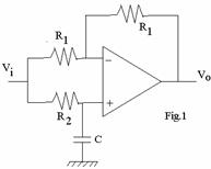
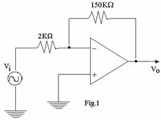
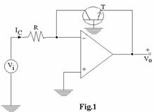
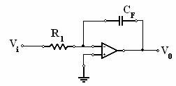
Q.1 Explain
Miller Integrator. What are the effects of the OP-AMP input offset voltage,
input bias and offset currents on the performance of Miller Integrator. (7)
Ans:
The circuit shown realizes the mathematical operation of
integration.
Writing modal equation at node (1)

Integrating both sides


Where vo(0) is the initial voltage on C1
therefore this is initial output voltage.
This circuit provides an output voltage that is proportional to
integration of the input voltage with vo being the initial
condition of integration and C1R1 the
integration time constant.
When vi = 0 the above integrator works as an open
loop amplifier. This is because the capacitor C1 acts as an
open circuit (XC1= ∞) to the input offset voltage vio.
Thus the input offset voltage vio and the part of input current
charging capacitor C1 produces the error voltage at the
output of the integrator. Therefore, in the practical integrator to reduce the
error voltage at the output, a resistor RF is connected in parallel
to capacitor C1.
Q.2 What is a
counter? How are counters broadly classified? Write at least two lines on
each such classification. (7)
Ans:
A sequential circuit that goes through a prescribed set of states
upon application of input pulses is called a counter.
Types
of Counters
(i)
Ripple Counters
·
Binary
·
BCD
(ii)
Synchronous Counters
·
Binary
·
BCD
(iii)
Ring Counter
Ripple counters are those, in which the change in output of one
counter flip flop triggers the next flip flop which further triggers the next
one, thus the effect of input pulses is rippled through. Binary counters of
this type cycle through the various binary codes.
BCD counters on the other hand cycle through the BCD code.
Synchronous counters act so that a common clock pulse triggers all the flip
flops at once. The ripple effect is not observed and all flip-flops flip or
flop simultaneously. Here also the Binary and BCD code cycle through in the
corresponding counters. In a ring counter, only one bit is high at a time and
the counters are connected in a loop. Thus a k flip flop ring counter has k
states.
Q.3 Draw the
circuit diagram of two stage CMOS op-amp configuration. What do you understand
by systematic output dc offset voltage? How can it be eliminated? (8)
Ans:
Unless properly designed, this CMOS OPAMP circuit exhibits a type of
input offset voltage that can be present even if all appropriate devices are
perfectly matched. This predictable systematic offset voltage at input causes
systematic output offset voltage.
It can be eliminated by sizing the transistors so as to satisfy following
constraint:

Q.4 Draw the
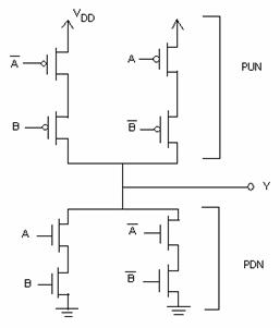
circuit diagram of a CMOS inverter and explain its operation. (6)
Ans:
CMOS Inverter: It is most widely used
in chip design. This operates with very little power loss. CMOS inverter has
good logic buffer characteristics as its noise margin in both low and high
states are large. CMOS does not contain any resistors which makes it more power
efficient. When Vin = VDD, Qn turns on and Qp
turns off therefore Vout = 0 volts (logic 0), and since transistors
are connected in series, the current ID is very small. When Vin
= 0V, Qp turns on and Qn turns off and Vout
= VDD (logic 1). So output is inverted version of input voltage.
Transfer characteristic of CMOS inverters.
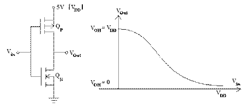
Q.5 The transfer
function of a two port network is given by  where
where  and
and  represent any impedances. Explain how
the following passive filters can be realized from this network.
represent any impedances. Explain how
the following passive filters can be realized from this network.
a)
Bandpass filter. (4)
b)
Notch filter. (5)
c)
All pass filter. (5)
Ans:
1) Putting Z1 = SL1+1/SC1 & Z2=R1
T(S) = 
2) Putting Z1=R1 & Z2 = SL1+1/SC1

3)Transfer function of All pass Filter
T(S) = 
Q.6 With proper diagram explain
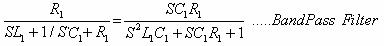
the operation of dual slope A/D converter and charge redistribution A/D
converter. Compare their advantages and disadvantages. (10)
Ans:
The charge redistribution A/D converter utilizes binary weighted
capacitor array, a voltage comparator and analog switches; control logic. Capacitor CT serves the purpose of terminating the capacitor array
making total capacitance of the array equal to desired value of 2C.
The operation has 3 phases: a) Sample phase, b) Hold phase c)
Charge- redistribution phase.
a)
Sample phase:
In this phase, switch SB is closed, thus connecting the top plate of
all capacitors to ground and setting V0 to zero. Meanwhile switch SA
is connected to analog input voltage VA which appears across all
capacitors resulting in a stored charge of 2CVA. Thus, a sample of VA
is taken and a proportionate amount of charge is stored on capacitor array.
b)
Hold phase:
In this phase, switch SB is opened and switches S1 to S5
and ST are thrown to the ground side. Thus top plates are open
circuited while bottom plates are grounded. Since no discharge path is
provided, capacitor charges remain constant, with total equal to 2CVA.
So, voltage at top plate becomes - VA. Finally SA is
connected to VREF .
c)
Charge-redistribution phase: In this phase, switch S1 is connected to VREF (through
SA).The circuit then consists of VREF, a series capacitor
C and a total capacitance to ground of value C. The capacitive divider cause of
a voltage increment of VREF/2 to appear on top plates. None if VA
is greater then VREF/2, the net voltage at the top plate will
remain negative which means that S1 will be left in its new position
as we move on the switch S2. If VA was smaller then VREF
/2, then the net voltage at the top-plate would become
positive. The comparator will detect this situation and signal the control
logic to return S1 to its ground position and then to move on to S2
Next, switch S2 is connected to VREF which
causes a voltage increment of VREF / 4 appear on top plate.
Digital output
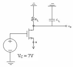
Q.7 Explain
the operation of sample & hold circuit. Discuss its applications. (4)
Ans:


Here, the MOSFET is used as a switch and OPAMP as a buffer. The
switch is put on by applying a positive pulse on the gate. The capacitor gets
charged with the required value with RC time constant. Sample & hold
circuit can be used to produce samples of analog voltage which can be used in a
analog to digital converter (ADC). The input voltage Vi to be
sampled is applied at the drain. When control voltage is high MOSFET is ON and
capacitor is charged up to the value of input signal, and the same voltage is
available at the output. When Vc is zero the MOSFET is OFF and acts as open
circuit. The only discharge path of capacitor is through OPAMP. However the
input impedance of voltage follower is very high, hence the voltage across
capacitor is retained.
WAVEFORMS
Q.8 What types of doping should be used in a switching diode. What is
reverse recovery time? (4)
Ans:
In switching diodes a lightly doped neutral region is made whose
length is shorter than a minority carrier diffusion length. In this case the
stored charge for forward conduction is very small since most of the injected
carriers diffuse through the lightly doped region to end contact. When such a
diode is switched to reverse conduction, very little time is required to
eliminate the stored charge in the narrow neutral region.
A second approach is to add efficient recombination centres to the
bulk material. For Si diode, Au doping is useful for this purpose. To a good
approximation the carrier the carrier lifetime varies with the reciprocal
center concentration.
The total time required for the reverse current to decay to 10% of
its maximum magnitude is defined as recovery time.
Q.9 Explain the operation of a MOSFET analog switch with suitable
circuit diagram. (6)
Ans:
 MOSFET as analog
switch: In applications where need arises to switch
analog signal, the switch is said to be analog switch. Following is a circuit
of analog switch using N MOS transistor
MOSFET as analog
switch: In applications where need arises to switch
analog signal, the switch is said to be analog switch. Following is a circuit
of analog switch using N MOS transistor


Fig (a)
Fig (b)
Fig (c)
Let input voltage VA be in the range of  5V. In order to keep
the substrate-to-source and substrate-to-drain pn junction reverse biased at
all times, the substrate terminal is connected to -5V. The control voltage Vc
is used to turn the switch on and off .Let us assume that the device has a
threshold voltage Vt=2V. Then in order to turn the transistor on
for all possible input signal levels the high value of Vc should
be +7V and to turn off transistor for all possible input voltage levels the low
value of Vc should be a maximum of -3V.
5V. In order to keep
the substrate-to-source and substrate-to-drain pn junction reverse biased at
all times, the substrate terminal is connected to -5V. The control voltage Vc
is used to turn the switch on and off .Let us assume that the device has a
threshold voltage Vt=2V. Then in order to turn the transistor on
for all possible input signal levels the high value of Vc should
be +7V and to turn off transistor for all possible input voltage levels the low
value of Vc should be a maximum of -3V.
MOSFET is a symmetrical device, with the source and the drain
interchangeable. The operation of the device as switch is based on this
interchangeability of roles. Whichever of the two terminals a and b is at
higher voltage acts as the drain. Thus if analog input voltage is positive say
+4V then terminal a acts as drain and b as source. Then the circuit takes the
form as shown in figure (b) above. The device will operate in triode region and
output voltage will be very close to the input analog signal level of +4v.On
the other hands if the input signal is negative say -4v then terminal b acts as
the drain. The circuit takes the form shown in figure (c). Again device
operates in triode region and V0 will be only slightly higher than
analog input signal level of -4V.
Q.10 What
property of Schottky diode make it suitable for fast switching? Explain . (4)
Ans:
The schottky barrier diode is formed by bringing metal into contact
with a moderately doped n-type semiconductor. In schottky diode current is
conducted by majority carriers. Thus it does not exhibit the minority-carrier
charge storage effect; as a result diodes can be switched on to off vice versa
much faster than is possible with p-n junction diode.
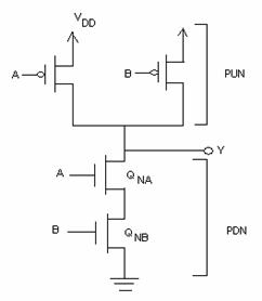
Q.11 Implement
the following Boolean expressions by synthesizing Pull up and Pull down
networks:
(i)
 . (4)
. (4)
(ii)  . (5)
. (5)
(iii)  . (5)
. (5)
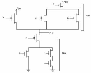
Ans:
(i)Y = 
Pull down network (PDN) can be synthesized by expressing  as function of un- complemented
variables. We consider input combination that requires Y to be low.
as function of un- complemented
variables. We consider input combination that requires Y to be low.
Y =
=  +
+

This requires that both A and B to be high. Thus PDN consists of two
NMOS transistors in series.
To synthesize Pull up network (PUN), we consider the input
combination that result in Y being high. From Y= , it requires that for Y to be high, A
or B to be low.
, it requires that for Y to be high, A
or B to be low.
(ii)
PUN Y = 
= 
= 
= 
=  ,
,
Y is high for A low or B low and either C or D low.
PDN
Y= 
For Y to be low, A should be high and simultaneously either B high
or C and D both high.
(iii) 
Q.12 Explain
the following logic families and compare their performances. (9)
(i)
ECL. (ii) TTL
Ans:
(i)ECL (Emitter Coupled Logic) is
recommended in high frequency applications where its speed is superior.
Justification:
1.
It is non saturated logic, in the sense that
transistors are not allowed to go into saturation. So, storage time delays are
eliminated and therefore the speed of operation is increased.
2.
Currents are kept high, and the output impedance
is so low that circuit and stray capacitances can be quickly charged and
discharged.
3.
The limited voltage swing. (i.e. the logic levels
are chosen close to each other)
Important features:
1. One advantage of differential input try in ECL
gates is that it provides common mode rejection – power supply noise common to
both sides of the differential configuration is effectively cancelled out.
2. Also, since the ECL output is produced at an
emitter follower, the output impedance is desirably low. As a consequence, the
ECL gates not only have a larger fan out but also are relatively unaffected by
capacitive loads.
(ii) TTL stands for “Transistor –
Transistor Logic”. It is the most popular logic family and also the most widely
used bipolar digital IC family. It uses transistors operating in saturated
mode. Good speed, low manufacturing cost, wide range of circuits and
availability in SSI and MSI are its merits.
The open collector arrangement is much slower than the totem pole
arrangement, because the time constant with which the load capacitance charges
in this case is considerably larger. (In the case of totem pole output, it is
active pull up. Thus the output rises fast). For this reason, the open
collector circuits should not be used in applications where switching speed is
a principal consideration.
Q.13 How
ECL and TTL logic families are interfaced with each other. (5)
Ans:
Interfacing of ECL and TTL with each other: In interfacing between
TTL and ECL gates, the logic levels between two systems are entirely different
therefore level shifting circuits are required to be used between these gates.
For TTL to ECL and ECL to TTL, two level translator IC’s are available– MC 10
H124.

The logic levels
of translator circuit are
VIH = 2V,
VIL = 0.8V
VOH = -0.98
v, VOL= -1.63V
For TTL IC we have
VOH = 2.4V and VOL = 0.4V. Comparing the O/P logic levels
of TTL and I/P logic levels of translator IC we find
VIH (Translator)
< VOH (TTL)
VIL
(Translator) > VOL (TTL)
This shows that
the I/P logic levels of translator are compatible with the O/P logic levels of
TTL
Similarly
VIH
(ECL) < VOH (Translator)
VIL (ECL) > VOL (TTL)

Q.14 With
a suitable circuit diagram explain how a four bit binary full adder works. How
this 4-bit adder can be used as substracter. (8)
Ans:
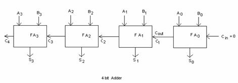
Operation: The first FA0 adding
the LSB, A0 and B0 is essentially a half adder whose sum
bit is  and
Cout=A0B0 since Cin is set to 0.
The Cout of the addition of LSB’s is carried over to the addition of
next bits i.e.A1,B1 which are added using a full adder,
FA1 This procedure continues with all the next adders being full
adders till the MSB’s, A3 and B3 .
and
Cout=A0B0 since Cin is set to 0.
The Cout of the addition of LSB’s is carried over to the addition of
next bits i.e.A1,B1 which are added using a full adder,
FA1 This procedure continues with all the next adders being full
adders till the MSB’s, A3 and B3 .
The final sum is S3S2S1S0 where
S3 is the MSB and So is the LSB.
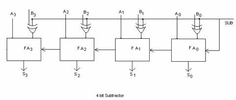
The subtraction is performed using two’s complement as  . If B=1, then Output
of XOR gate is 0. If B=0, then output is 1. Thus a four bit adder is converted
into a subtractor by connecting bits of input number B as one of the input of
XOR gate. The second input of XOR gate is kept as logic 1. Now when I/P B=0 then
output of XOR gate is 1 and if B=1 then output is 0. Now 1 is added to this
complimented number so that we get
. If B=1, then Output
of XOR gate is 0. If B=0, then output is 1. Thus a four bit adder is converted
into a subtractor by connecting bits of input number B as one of the input of
XOR gate. The second input of XOR gate is kept as logic 1. Now when I/P B=0 then
output of XOR gate is 1 and if B=1 then output is 0. Now 1 is added to this
complimented number so that we get . These input’s are applied to the B
input of the adder and at the output, we will get the output as
. These input’s are applied to the B
input of the adder and at the output, we will get the output as
Q.15 Explain
the operation of a BCD to decimal decoder. (6)
Ans:
BCD to Decimal DecoderThis is a type of
decoder which decodes the BCD input in decimal. There are four input’s and ten output’s
and depending on the input combinations the corresponding output line is high.


 W X
Y Z Do D1 D2 D3 D4 D5 D6 D7 D8 D9
W X
Y Z Do D1 D2 D3 D4 D5 D6 D7 D8 D9
0 0 0 0 1 0 0 0 0 0 0 0 0 0
0 0 0 1 0 1 0 0 0 0 0 0 0 0
0 0 1 0 0 0 1 0 0 0 0 0 0 0
0 0 1 1 0 0 0 1 0 0 0 0 0 0
0 1 0 0 0 0 0 0 1 0 0 0 0 0
0 1 0 1 0 0 0 0 0 1 0 0 0 0
0 1 1 0 0 0 0 0 0 0 1 0 0 0
0 1 1 1 0 0 0 0 0 0 0 1 0 0
1 0 0 0 0 0 0 0 0 0 0 0 1 0
1 0 0 1 0 0 0 0 0 0 0 0 0 1
Now Ten K- maps are required to get the ten outputs from D0
to D9. Instead of making ten K-maps, we make only one K-map and make
the entries as follows:
While solving for
D0 consider D0 as high and all other D’s as zero. Some of
the functions are
D0 = w’x’y’z’
D1 = w’x’y’z
D2 = x’yz’
(by combining with don’t care at 1010)
D3 = x’yz
(by combining with don’t care at 1011)
D4 = xy’z’
D5 = xy’z
D6 =
xyz’
D7 =
xyz
D8 = wz’
(three don’t cares)
D9 =
wz (three don’t cares)
Now this can be
implemented using AND gates
Q.16 Explain
the following with timing diagram.
(i)
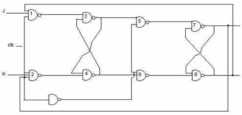
JK flip-flop. (7)
(ii)
Clocked SR flip-flop. (7)
Ans:
(i) JK Flip-flop: JK flip flop is a
single bit storage device which came into the picture to overcome the
disadvantages of RS flip flop. This disadvantage was Race-around condition. The
following excitation table shows what flip-flop inputs are required in order to
make a desired state change.
Q(t)
|
Q(t+1)
|
J
|
K
|
Operation
|
|
0
|
0
|
0
|
x
|
No
change/reset
|
|
0
|
1
|
1
|
x
|
Set/complement
|
|
1
|
0
|
x
|
1
|
Reset/complement
|
|
1
|
1
|
x
|
0
|
No
change/set
|
Truth
Table
J
|
K
|
Q(t+1)
|
Operation
|
|
0
|
0
|
Q(t)
|
No
change
|
|
0
|
1
|
0
|
Reset
|
|
1
|
0
|
1
|
Set
|
|
1
|
1
|
Q’(t)
|
Complement
|
Logic Symbol
JK flip-flops are
good because there are many don’t care values in the flip-flop inputs, which
can lead to a simpler circuit.
Circuit
of JK Flip Flop
Example waveforms for
J K Flip Flop
(ii) Clocked S/R flip flop
Characteristic
table
clk S R
Qt + 1
0 X X Qt No Change
1 0 0 Qt No Change
1 0 1 0
1 1 0 1
1 1 1 Forbidden (?)
There are two inputs S(Set) and R (Reset). When clock is enabled
(clk=1) and both the inputs are 0 then flip flop does not change the state. S=1
and R=0 sets the Q output, whereas S=0, R=1 resets Q output. S=R=1 input
condition is forbidden as both output Q and  will try to become 1. This is regarded
as invalid circuit operation. when clk = 0 output will always retain the
previous state.
will try to become 1. This is regarded
as invalid circuit operation. when clk = 0 output will always retain the
previous state.
Characteristic equation for RS flip flop is
Q t+1 = (S + Qt)
Qt)
Timing
wave form for SR flip-flop
Q.17 Write short notes on any TWO of the
following:
(i)
RAM & PROM.
(ii) Seven segment display system.
(iii) Shift register.
(7+7)
Ans:
(i) RAM and PROM
A memory unit is a collection of storage cells together with
associated circuits needed to transfer information in and out of the device.
The time it takes to transfer information to or from any desired random
location is always same, hence the name RAM(Random Access Memory). It is
used for storing temporary data as it is volatile. The variables required for a
particular program are stored. Here RAM can perform both read and write
operations. Therefore all the variables during the ALF are stored here. The
static RAM (SRAM) consists of internal latches that store the binary
information. The stored information remains valid as long as power is there. The
dynamic RAM stores information in the form of charges on capacitor. The
capacitors are provided inside the chip by MOS transistors. The stored charge
tends to get discharged with time and the charge has to be periodically
refreshed.
DRAM offers reduced power consumption and larger storage capacity in
a single memory chip. SRAM is easier to use and has shorter read and write
cycles.
When production in small quantities is required a PROM or
programmable read only memory is used. When ordered PROM units contain all the
fuses intact giving all 1’s in the bits of stored words. The fuses in PROM are
blown using application of a high voltage pulse to the device through a special
pin. A blown fuse gives a binary ‘0’ state. This allows the user to program it
in the lab. Special programmes are used for this. The hardware procedure for
programming ROMs is irreversible & once programmed the pattern is
irreversible. The EPROM is erasable and can be restructured. When EPROM is
placed under special ultraviolet light for a given period of time, the short
wave radiations discharge the internal floating gates. But individual bits
can’t be reprogrammed as in case of EEPROM. The programming takes lot of time,
about 30 min and the whole ROM is reprogrammed. The device has to be removed from
its socket to reprogram it.
(ii) Seven Segment display systems:
This system
accepts BCD numbers as input and there are seven outputs which are connected to
seven LED’s. According to the display required corresponding LED’s are made
high. For example if ‘Two’ is to be displayed then a, b, e, d and g should be
high and others are kept-low.
BCD to Seven
segment
Display
|
|
|
W
|
X
|
Y
|
Z
|
a
|
b
|
c
|
d
|
e
|
f
|
g
|
|
0
|
0
|
0
|
0
|
1
|
1
|
1
|
1
|
1
|
1
|
0
|
|
0
|
0
|
0
|
1
|
0
|
1
|
1
|
0
|
0
|
0
|
0
|
|
0
|
0
|
1
|
0
|
1
|
1
|
0
|
1
|
1
|
0
|
1
|
|
0
|
0
|
1
|
1
|
1
|
1
|
1
|
1
|
0
|
0
|
1
|
|
0
|
1
|
0
|
0
|
0
|
1
|
1
|
0
|
0
|
1
|
1
|
|
0
|
1
|
0
|
1
|
1
|
0
|
1
|
1
|
0
|
1
|
1
|
|
0
|
1
|
1
|
0
|
1
|
0
|
1
|
1
|
1
|
1
|
1
|
|
0
|
1
|
1
|
1
|
1
|
1
|
1
|
0
|
0
|
0
|
0
|
|
1
|
0
|
0
|
0
|
1
|
1
|
1
|
1
|
1
|
1
|
1
|
|
1
|
0
|
0
|
1
|
1
|
1
|
1
|
1
|
0
|
1
|
1
|
Truth table
The input combinations 1010 to 1111 are invalid combinations so they
can be treated as don’t care conditions while solving the K-maps. Now seven
K-maps for a, b, c, .... g are solved in terms of I/P’s BCD number
wxyz and implemented using AND-OR or NAND-NAND gates.
(iii) Shift
Register: A register is a group of flip flops. Each
flip flop is capable of storing one bit of information. An n bit register is
capable of storing n bite of binary information. A register capable of shifting
its binary information in one or both direction is called a shift register. It
consists of a chain of flip flops in cascade, with the output of one flip flop
connected to the input of the next flip flop. All flip flops receive common
clock pulses, which activate the shift from one stage to the next. 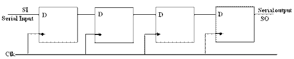
This is a 4 bit
shift register. The output of a given flip – flop is connected to the D input
of the flip – flop at its right. Each clock pulse shifts the contents of the
register one bit position to the right. The serial input determines what goes
into the left most flip flop during the shift. Serial output is taken from the
output of the right most flip flop. This is a right shift operation. We can
also construct a left shift register where inputs are inserted from right and
output is taken from the left. If the flip flop outputs of a shift register are
accessible then information entered serially by shifting can be taken out in
parallel manner from the flip flop’s. If a parallel load capability is added to
shift register then data entered in parallel can be taken out in serial fashion
by shifting the data stored in the register.
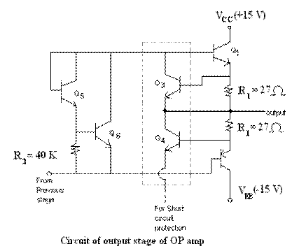
Q.18 What
are the requirements of the output stage of an OPAMP? Write the circuit of the
output stage of the  OPAMP. (7)
Ans:
Requirements of the output stage of an OPAMP:
·
Should have low output impedance. Should be able
to supply relatively large load currents without dissipating large amount of
power.
·
Should have a considerably large current gain so
as to provide power amplification.
·
Should be properly designed so as to have
minimum parasitic capacitances.
Circuit for the output stage of OPAMP
·
Output stage is class AB push-pull stage with Q1
& Q2 (Minimizing crossover distortion)
·
Q3 & Q4 provide means
of short circuit protection when o/p is a ceidently connected to grand.
·
Q5 & Q6 help in
biasing the transistors to work in class AB mode.
·
Output impedance 75 r
·
Output voltage swing-: Vomax = VCC
- Vcesat –V BE Vomin = - VEE +V
CESAT + 2VEB.
·
Max output current (sinking or sourcing) = 20 MA
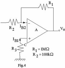
Q.19 Why
do you require dc level shifting in OPAMPs? What are the requirements of the
level shifting stage? Write a typical circuit for measuring the input bias
current of an OPAMP and explain the procedure for measurement. (9)
Ans:
DC level shifting in OPAMPS
Because of the multiple gain stages used in an OPAMP, the DC level
needs to be restored before signal can be fed into the next gain stage. Thus DC
level shifting is required.
Requirements for level shifting stage:-
·
Should bring the dc level of the signal down to
zero without affecting the ac component of the signal.
·
Should have high input impedance and low output
impedance to the a.c. component as it behaves as an intermediate stage coupling
two stages in an OPAMP.
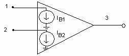
Circuits for measuring input bias current of an OPAMP are:
Assumptions
-Vi0 = 0
IB1 = IB2 =IB– Ii0
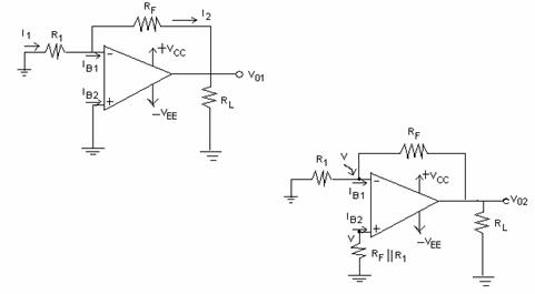
Procedure:
·
Measure Vo1

·
Measure Vo2

From (i)
From (ii) and (iii) 
Q.20 What
is an active filter? What is the role of the amplifier of the active filter?
What are the limitations of active filters? (9)
Ans:
Active Filters
A filter comprising of active elements such as OPAMPS, current
conveyors etc along with passive elements so as to provide amplification along
with filtering are called active filters.
Role of Amplifier is an active filter:
a)
To provide a pass band gain.
b)
To provide buffering action to isolate the
filter with the output stage.
c)
Improve the Q factor of the filter by using
+ve feedback and improve tunability
d)
To realize universal filters
Limitations
of active filters:
·
Circuit more complex than conventional passive
filters. Problems of instability and ringing.
·
Dependence of filter parameters on device
parameters which are difficult to control (like gain of OPAMP) and sensitive to
temperature variations.
·
Limited in usage up to medium frequencies.
Difficult to realize an active filter at VHF owing to the limitation of
OPAMPS.
Q.21 Design
a combinational circuit that accepts a 3-bit number as input and generates an
output binary number equal to the square of the input number using ROM. (9)
Ans:
The maximum no that can be at
the o/p is (7) 2 =49 = 110001
Thus
the output will be of 6 bit max
|
x
|
y
|
z
|
A
|
B
|
C
|
D
|
E
|
F
|
Decimal
|
|
0
|
0
|
0
|
0
|
0
|
0
|
0
|
0
|
0
|
0
|
|
0
|
0
|
1
|
0
|
0
|
0
|
0
|
0
|
1
|
1
|
|
0
|
1
|
0
|
0
|
0
|
0
|
1
|
0
|
0
|
4
|
|
0
|
1
|
1
|
0
|
0
|
1
|
0
|
0
|
1
|
9
|
|
1
|
0
|
0
|
0
|
1
|
0
|
0
|
0
|
0
|
16
|
|
1
|
0
|
1
|
0
|
1
|
1
|
0
|
0
|
1
|
25
|
|
1
|
1
|
0
|
1
|
0
|
0
|
1
|
0
|
0
|
36
|
|
1
|
1
|
1
|
1
|
1
|
0
|
0
|
0
|
1
|
49
|
From the truth
table we can see that F is always equal Z and output E is always 0; so this is
a constant. So we need to generate only 4 outputs with ROM. So minimum size of ROM needed must have 3 inputs and 4 outputs. Three inputs specify
eight words so the ROM must be of size 8X4. x, y, z are three inputs and A, B,
C and D are four outputs of the ROM.
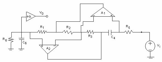
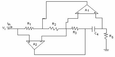
Q.22 What are the advantages of switched capacitor filters? Design a
switched capacitor integrator for critical frequency of 20 Hz. Assume
frequency of clock as 2 KHz. Compare with an RC integrator. (10)
Ans:
Advantages of Switched capacitor filters:
·
No need of resistances which occupy a large
space on chip and difficult to fabricate.
·
Easy to simulate large value of resistances with
available capacitances by changing the clock frequency.
·
Easy to tune the circuit electronically as
resistance and hence the filter parameters such as cut off frequency and
Q-factor depend on the clock frequency.
·
Suited for large scale integration of circuits
for analog application.
An RC
integrator is given below and transfer function is given as


The resistor R can
be replaced by a switched capacitor C1 as shown below.
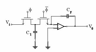
where fck = clock frequency
|
|

Design: given fo = 20Hz, fck = 2 KHz.
So we choose CF
= 15.9 pF and C1 = 1 pF.
For RC integrator
if we take R1 = 10 KΏ then C=0.79µF. This is a large value of
capacitance.
If we choose small
value of capacitance let us say 10nF then R1=0.795MΏ.
Fabrication of high value of R and C is not practical for a monolithic circuit,
so switched capacitance is a better choice.
Q.23 Write
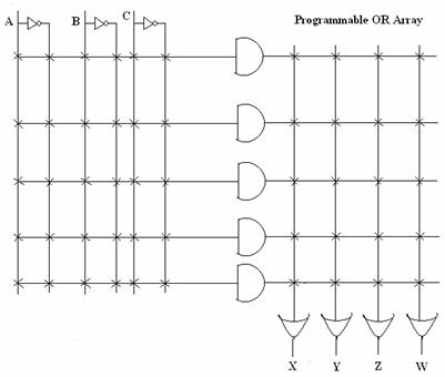
the general structure of a PLA. Write the logic diagram of a general  PLA. How are PLAs
characterised? (6)
PLA. How are PLAs
characterised? (6)
Ans: Input
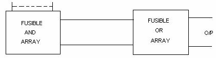
General structure of PLA
PLAs along with PAL & ROM are included in the more general
classification of IC’s called Programmable Logic Devices (PLDs).
In each case input signals are presented to an array of AND gates
while the outputs are taken from an array of OR gates. The PLA is much more
versatile than PROM & PAL since both its AND gate array & OR gate array
are fusible linked and programmable.

Q.24 Write
the logic diagram, truth table, and the logic symbol of a
positive-edge-triggered T flip-flop. (3)
Ans:
Positive edge triggered T-Flip
Flop.
Logic Diagram:
Truth
table
Q(t=o)
T Q(t=1)
0 0 1
0 1 1
1 0 0
1 1 0
Characteristic
equation : Q (t = 1) = TQ’ + T’Q = T +
Q
Logic Symbol: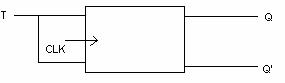
Q.25 Briefly
explain the operation of an antilog amplifier circuit that uses two OPAMPS. (6)
Ans: Antilog amplifier

From the figure above

Since the base of Q1 is tied to ground  , therefore

VB is the base voltage of Q2 and is output
from the R2, RTC voltage divider.

The voltage at the emitter of Q2 is

On substitution, we get

But the emitter of Q2 is VA thus

Where 
Q.26 Briefly explain how the speed of a transistor response can be
improved by preventing the transistor from going into saturation. (4)
Ans:
The storage delay time can be reduced considerably by
preventing the transistor from going into saturation. One way of achieving this
is to connect a Schottky diode between the base and collector of the
transistor. When the transistor is in the active region, the diode D is reverse
based. The diode conducts when the base-collector junction voltage falls to
about 0.4v and does not allow the collector junction voltage to fall lower than
0.4V below the base voltage. Hence the collector junction is not sufficiently
forward-biased and the transistor is thus prevented from entering into
Saturation.
Q.27 Comment
on the switching speeds in FET devices. (4)
Ans:
Comment on the switching speeds in FET devices:
FET devices are slower in terms of operating speed and are
susceptible to static charge damage. For MOS logic, tpd =50 ns. The
propagation delay associated with MOS gate is large (50ns) because of their
high output resistance  and capacitive loading present at the
driven gates.
and capacitive loading present at the
driven gates.
Thus, if we apply a square pulse at the gate of an FET, the gate
voltage takes some time to rise due to the input capacitance & thus
switching becomes slower.
Q.28 What are the advantages of CMOS gates? Briefly explain an NMOS
two-input NAND gate. Assume that positive logic is intended. What is ‘SOS’ as
used in IC technology? (8)
Ans:
The CMOS logic family uses both P and N channel MOSFETs in the same
circuit to realize several advantages over PMOS and NMOS families. The CMOS
family is faster and consumes less power than other MOS families. CMOS devices
can be operated at higher voltage resulting in increased noise immunity.
NMOS and input NAND gate
The following fig shows two input NMOS NAND gate & its
equivalent circuit for different possible combinations of inputs in terms of
resistance values of transistors in ON and OFF positions.

(a) 2 I/P NMOS (b) A
LOW (c) A LOW (d) A HIGH
NAND GATE B
HIGH B HIGH B LOW
‘SOS’ is a relatively new IC fabrication technology named as
“silicon-on-Saphire”
Q.29 What
is TTL? Illustrate the simplest and most elemental form of a TTL gate by a
sketch and explain its operation when the input to the gate is ‘HIGH’ and
‘LOW’. What is the main reason for the speed limitation of TTL? How can this
be eliminated? (8)
Ans:
TTL stands for “Transistor – Transistor Logic” It is the most popular logic family and also the most widely used
bipolar digital IC family. It uses transistors operating in saturated mode.
Good speed, low manufacturing cost, wide range of circuits and
availability in SSI & MSI are its merits.
Open collector TTL inverter.
When the input is high, the diode D is reverse biased & thus
OFF. Moreover, transistor Q1 is in cut off mode. Thus, the current
through R1 suffers a small voltage drop across the base – collector
junction of Q1 and hence switches on Q2. The emitter
current of Q2 (which will be (β+1) times the base current)
switches transistor Q3 ON. Since the emitter of Q3 is
grounded, the collector is also at near ground potential, thus low. But when
the input is low, the diode D is F/B and Q1 is ON. The enough base
drive is not available for Q2 to turn ON. As a result Q3
is also OFF. Due to this, the collector of Q3 is floating. To
prevent this, we have a passive pull up resistor, which takes the O/P to +5V in
case Q3 is off.

Open collector TTL inverter
The open collector arrangement is much slower than the totem pole
arrangement, because the time constant with which the load capacitance charges
in this case is considerably larger. (In the case of totem pole output, it is
active pull up. Thus the output rises fast). For this reason, the open
collector circuits should not be used in applications where switching speed is
a principal consideration.
Q.30 In what type of applications is the ECL recommended? Justify its
suitability in such application. Write the circuit of a 3-input ECL OR/NOR gate
and mention its features. What is its logic symbol?
(8)
Ans:
ECL is recommended in high frequency applications where its speed is
superior.
Justification:
a.
It is not saturated logic, in the sense that
transistors are not allowed to go into saturation. So, storage time delays are
eliminated & therefore the speed of operation is increased.
b.
Currents are kept high, and the output impedance
is so low that circuit & stray capacitances can be quickly charged and
discharged.
c.
The limited voltage swing that is the logic
levels are chosen clock to each other.

Circuit of ECL OR/NOR Gate
Important features:
1)
One advantage of differential input circuit in
ECL gates is that it provides common mode rejection – power supply noise common
to both sides of the differential configuration is effectively cancelled out.
2)
Also, since the ECL output is produced at an
emitter follower, the output impedance is desirably low. As a consequence, the
ECL gates not only have a larger fan out but also are relatively unaffected by
capacitive loads.
(2) I/P ECL OR/NOR gate
(3) Symbol
Q.31 Two
binary numbers  and
and

 are to be added.
Draw the scheme of a parallel binary adder consisting of half adders and
explain its operation. (7)
are to be added.
Draw the scheme of a parallel binary adder consisting of half adders and
explain its operation. (7)
Ans:
HA Cascaded with another
forms of FA (Full Adder)
Operation:
The first FA0 adding the LSB, A0 and B0 is
essentially a half adder whose sum bit is A0 + B0 and Cout
since Cin is set to 0 . The Cout of the addition of LSB’s
is carried over to the addition of next bits i.e.A1,B1
which are added using a full adder, FA1 This procedure continues
with all the next adders being full adders till the MSB’s, A3 &
B3 .
The final sum is S4S3S2S1S0
Where S4 is the MSB and so is the LSB.
Q.32 Explain
how an S-R flip-flop can be converted into a J-K flip-flop. (5)
Ans:
Here, we are actually given an SR flip-flop but we have to make it
function like a JK Flip-flop i.e. to say for all possible combination of Input
to SR FlipFlop, the Outputs should be matching with that of a JK flip-flop.
Logic Diagram
Conversion
Table
|
J
|
K
|
Qn
|
Qn+1
|
S
|
R
|
|
0
|
0
|
0
|
0
|
0
|
X
|
|
0
|
0
|
1
|
1
|
X
|
0
|
|
0
|
1
|
0
|
0
|
0
|
X
|
|
0
|
1
|
1
|
0
|
0
|
1
|
|
1
|
0
|
0
|
1
|
1
|
0
|
|
1
|
0
|
1
|
1
|
X
|
0
|
|
1
|
1
|
0
|
1
|
1
|
0
|
|
1
|
1
|
0
|
0
|
0
|
1
|
Q.33 Briefly
explain the operation of a 4-to-1 line multiplexer using AND-OR logic. (4)
Ans:
A multiplexer or a data selector is a N to 1 device with N Input
lines and 1 Output line. The select line decides which of the Input lines sends
its data to the Output line.
As per the truth table, it can be easily deduced that

Truth table
|
S1 S0
|
Output
|
|
0 1
|
|
D0
|
|
0 1
|
|
D1
|
|
1 0
|
|
D2
|
|
1 1
|
|
D3
|
Q.34 What
is a programmable logic device? Illustrate by a neat sketch the configuration
of AND and OR arrays for a PAL with 5 inputs, 8 programmable AND gates, and 4
fixed OR gates. (6)
Ans:
A PLD is an IC that is user configurable and is capable of
implementing logic functions. It is an LSI that contains a regular structure
and allows the designer to customize it for any specific application. It is
programmed by the user to perform a function required for his application.
Q.35 List
the advantages of a programmable logic device over fixed function ICs. (4)
Ans:
The advantages of PLD’s over fixed function ICs are
(i)
Reduction in board space requirement.
(ii)
Reduction in power requirement.
(iii)
Design security.
(iv)
Compact circuitry.
(v)
Higher switching speed.
Q.36 Write the basic structure of a sequence generator using a shift
register and design a sequence generator to generate the sequence 1101011. (6)
Ans:
Sequence generator:
This circuit generates the prescribed sequence of bits in
synchronizing with clock. The output y of the next state decoder is a function
of QN-1 QN-2 ....Q1 Q0.
Design: The minimum no of flip flops, N1
required for generating a sequence of length S is given by S ≤ 2N-1
In this case S=7 thus the minimum value of N=3.
|
No. of clock pulse
|
State table
|
|
Q2
|
Q1
|
Q0
|
|
1
|
 1 1
|
   1 1
|
1
|
|
2
|
1
|
 1 1
|
1
|
|
3
|
0
|
  1 1
|
1
|
|
4
|
 1 1
|
0
|
1
|
|
5
|
 0 0
|
 1 1
|
0
|
|
6
|
 1 1
|
 0 0
|
1
|
|
7
|
1
|
1
|
0
|
Q2 is given sequence. Q1 and Q0 are
same sequence delayed by 1 and 2 clock pulses respectively since all the state
in the table are not distinct so N=3 is not sufficient.
Therefore we take N=4. Truth table of sequence generator (N=4)
|
No. of CLK pulses
|
Flip Flop Outputs
|
Serial Input
|
|
Q3
|
Q2
|
Q1
|
Q0
|
|
1
|
1
|
1
|
1
|
0
|
1
|
|
2
|
1
|
1
|
1
|
1
|
0
|
|
3
|
0
|
1
|
1
|
1
|
1
|
|
4
|
1
|
0
|
1
|
1
|
0
|
|
5
|
0
|
1
|
0
|
1
|
1
|
|
6
|
1
|
0
|
1
|
0
|
1
|
|
7
|
1
|
1
|
0
|
1
|
1
|
|
---------
|
-------------
|
-----------------
|
-----------
|
---------------
|
------------
|
|
1
|
1
|
1
|
1
|
0
|
1
|
|
2
|
1
|
1
|
1
|
1
|
0
|
|
3
|
0
|
1
|
1
|
1
|
1
|
|
*
|
1
|
0
|
1
|
1
|
0
|
|
*
|
0
|
1
|
0
|
1
|
1
|
|
*
|
1
|
0
|
1
|
0
|
1
|
The last column gives the required serial input for getting the
desired change of state when a clock pulse is applied. This is obtained by
assuming D flip-flop and looking at the Q3 output. The K map of Y
for inputs Q3 Q2 Q1 Q0 gives Y =  +
+  +
+ 
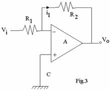
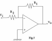
Q.37 Derive
an equation for the closed loop gain of an operational amplifier circuit shown
in Fig.5 if the open loop gain of the op amp is A. (4)
Ans:
Let the voltage at node 1 be V
Now By KCL at node 1, we have:-
 (As
current entering the OPAMP is O)
(As
current entering the OPAMP is O)
 (1)
(1)
But, By OPAMP equation, we have
Vo2 = A(-V+0)
Vo2 = -A×V (2)
From (1) & (2) ,
V02 =-A 
=V02 [( R1+R2) +AR2]
= -
=
Q.38 Explain
the meaning of the terms slew rate, input offset voltage, input bias current
and input offset current. (8)
Ans:
(i)
Slew Rate:- It is
defined as the maximum rate at which the output voltage of an OPAMP can change
It is expressed in V per m sec.
For mA741, \slew rate (S) = 0.5
V/m
sec.
It is a large
signal phenomenon and occurs mainly due to the input stage of the OPAMP going
into saturation. This happens when a relatively large signal is applied at the
input terminals (signal > 2VT in magnitude).
(ii)
Input offset voltage:- Due to mismatch in the 2 transistors forming the differential
stage of the input part of an OPAMP, a slight output voltage appears even when
the applied input is 0. This output voltage divided by the closed loop gain of
the OPAMP gives a voltage corresponding to the input terminals which when
balanced by an equal & opposite voltage would lead to the output voltage
being 0. This voltage is termed as input offset voltage.
(iii)
Input bias current:- The base currents of the two transistors constituting the
differential input stage of an OPAMP are termed as input bias currents.
(iv)
Input offset current :-
·
Due to mismatch in 2 input transistors, the base
currents are not same.
·
This mismatch in base current leads to an output
offset voltage being developed.
·
The difference in the base currents of the two
input transistors is termed as input offset current.
Q.39 Write
briefly on instrumentation amplifier. (4)
Ans: Instrumentation Amplifier
·
Used to amplify signals from transducers; often
constitute the pre-amplification stage.
·
High gain with minimal loading.
·
Difference between signals is amplified and
converted into a single ended output that can be used for further processing
the signal.
·
Robust amplifier and not affected by changes in
device parameters, temperature etc.
Q.40 What
is a digital magnitude comparator? With a circuit diagram that uses
exclusive-NOR gate, AND gates and inverters, explain the operation of a
single-bit magnitude comparator. (7)
Ans:
The
truth table of XNOR ie :
A B Y
0 0 1
1 0 0
0 1 0
1 1 1
To compare two
bits A and B, we must first find if they are equal, which can be done by
passing them through a XNOR, if output is 1 , then they are equal :
Now we complement ‘A’ and take
AND with ‘B’ if output is high, then B>A
Now we complement ‘B’ and take
AND with ‘A’ if output is high then A>B
The
complete circuit:
Q.41 Plot the response of a typical low pass Butterworth
filter and explain the response by identifying the different parameters. (5)
Ans:
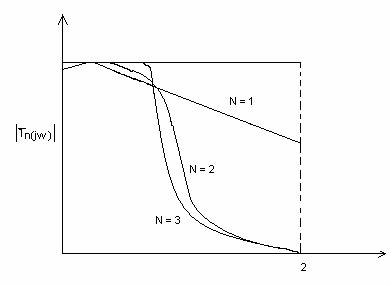
Characteristics of Butter
worth Response
1.
The Butterworth filter is an all pole filter; it
has zeros only at infinity (w® ∞).
2.
| Tn
(j0) | =1 for all n. This is a consequence of normalization.
3.
| Tn (j1) | =
4.
For large w, | Tn (jw) | exhibits n-
pole roll off that is the attenuation increases by 20n dB/decade.
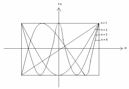
Q.42 Sketch
the transmission characteristics of an even and odd order Chebyshev low pass
filter and identify the important parameters. (5)
Ans:
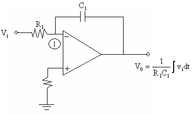
Q.43 Describe
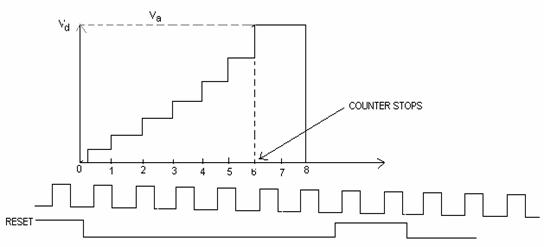
the counting type analog to digital converter with the help of a block diagram.
(12)
Ans:
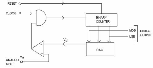
A 3-bit counting type ADC is shown in the figure above. The counter
is reset to zero count by the reset pulse. Upon the release of RESET the clock
the binary counter counts pulses. These pulses go through the AND gate which is
enabled by the voltage comparator high output. The number of pulses counted
increases with time. The binary word representing this count is used as the
input of a D/A converter whose output is a staircase of the type as in Figure.
The analog output Vd of DAC is compared to the analog input Va
by the comparator. If Va>Vd the output of the
comparator becomes high and the AND gate is enabled to allow the transmission
of clock pulses to the counter when Va<Vd, the output
of the comparator becomes low and the AND gates is disabled. This stops the
counting at the time Va £ Vd and the digital output of the
counter represents the analog i/p voltage Va. For a new value of
analog input Va, a second reset pulse is applied to clear the
counter.
Q.44 Explain the meaning of the terms conversion time and resolution of
an analog to digital converter. (4)
Ans:
Resolution: The resolution of a converter is the smallest change in the voltage
that may be produced at the output or input of the converter. In short, the
resolution is the value of LSB,
Resolution
(in volts) =  increment
The resolution
of A/D is defined as the smallest change in analog input for a one bit change
at the output.
Conversion
time: This is defined as conversion time = 
Where
n = number of bits.
f
= The frequency at which counter is operating
Q.45 Explain
the use of Schottky barrier diode in increasing the speed of switching. (4)
Ans:
The schottky barrier diode is formed by bringing metal into contact
with a moderately doped n-type semiconductor. In schottky diode current is
conducted by majority carriers. Thus it does not exhibit the minority-carrier
charge storage effect, as a result diodes can be switched on to off vice versa
much faster than is possible with p-n junction diode.
Q.46 Explain
the operation of BJT as a switch. (6)
Ans:
The speed at which a BJT can change its logic states is limited by
the delays of the transistor in switching between saturation and cut off modes
of operation. When the transistor is operating in the cut off mode, the emitter
base junction is 0 or reverse bias. As input voltage changes in forward
direction, base current increases. The collector current however does not
attain its saturation values instantaneously. Because the emitter base junction
transition capacitance must be charged to forward bias voltage. As the EBJ
becomes forward biased, the junction capacitance becomes predominantly
diffusion capacitance which controls the collector current. This contributes to
the delay time td. Once the transistor is brought from cut off to
active mode, the collector current begins to increase. Now the forward bias
diffusion capacitance at EBJ charges exponentially while IC rises as
βIB and reaches
its maximum of Icsat. The time taken in reaching Icsat is
tr. The sum of delay and rise time is the turn on delay of BJT. The
delay in turn off process of the transistor is caused primarily by the removal
of the excess minority carriers in the base region. When input voltage switches
from VH to VL, the collector current continues at its
saturation level until the excess charge is removed from the base region. The
storage or saturation delay is the interval during which Ic remains
at Icsat. The fall time of the collector current during which
transistor goes from active to cut off mode, is called tf. The sum
of storage and fall time is turn off delay.
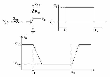
Q.47 The voltage shown in Fig.6 on the left is in applied to the circuit
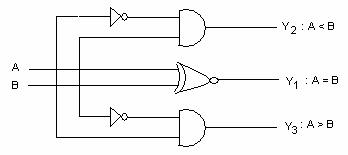
on the right. Sketch the output voltage as a function of time and explain how
you get that particular output. 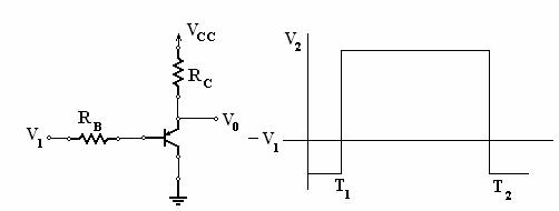 (6)
(6)
Ans:
In the given circuit when VI = -V1 then BE
function is reverse based and because of +Vcc, CB function is also
reverse biased. Thus the device is in cut off mode and the output voltage V0
is VCC. When input VI is V2 volts then
both the junctions are forward biased and transistor is in saturation mode. The
output voltage will be equal to V0 =V sat ≈0.2 V.
The slope is because of the switching delay i.e. switching from cut
off to saturation and from saturation to cut off respectively.
Q.48 Explain different TTL logic families and compare their performance. (4)
Ans:
The
different TTL Logic Families can be compared in the following table.
|
Logic Family
|
Prefix
|
Fan-out
|
Power dissipation
(mW)
|
Propogation.Delay
(ns)
|
Speed-Power product
|
|
Standard
|
74
|
10
|
10
|
9
|
90
|
|
Low Power
|
74 L
|
20
|
1
|
33
|
33
|
|
High Speed
|
74 H
|
10
|
22
|
6
|
132
|
|
Schottky
|
74 S
|
10
|
19
|
3
|
57
|
|
Schottky Low Power
|
74 LS
|
20
|
2
|
9.5
|
19
|
|
Advanced Schottky
|
74 AS
|
40
|
10
|
1.5
|
15
|
|
Advanced Low power Schottky
|
74 ALS
|
20
|
1
|
4
|
4
|
Q.49 Draw
a basic ECL logic NOR gate, and explain its operation. (12)
Ans:

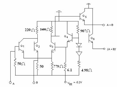
ECL NOR GATE
The working is very obvious, if any input is high (-0.8V) then the
corresponding transistor is turned on and Q3 is turned off. This
causes a voltage of -1.6V to appear at emitters of both of the transistors Q1
& Q2 Since VBB = -1.3v1 there is only a
drop of 0.3V at VBE of Q5 , hence it is in cut–off. Current
in the 220 Ω resistance flows through the conducting transistor and the
output of Q6 is low.
Now if both inputs are low, only Q3 will conduct, and Q1
& Q2 will be cut off this is because emitters will be at -2.1 V and each
transistor has its base at -1.8V hence drop is only 0.3V hence they are in
cut-off. In this situation current through the 220 W resistance flows out
through Q6 and O/P is high.
Truth Table:

 A B Y
A B Y
0 0 1
1 0 0
0 1 0
 1 1 0
1 1 0
Q.50 Design
a 1 bit digital comparator using basic logic gates to get three different
outputs and draw the circuit diagram. Using this, design a four bit
comparator. (12)
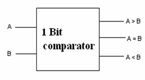
Ans: 1
bit comparator:
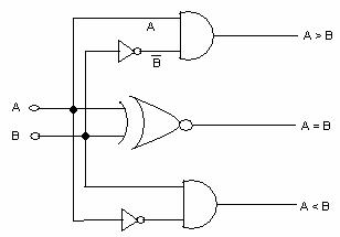
Using
this to get 4-bit comparator, we represent 1 bit comparator as:
Now A0A1A2A3
and B0B1B2B3 are the words to be
compared.
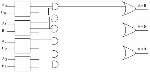
Though the circuit looks complex, it is very simple. The word A is
greater than B only if Ao > Bo or if Ao = Bo
and A1>B1 or Ao
= Bo and A1 = B1 and A2
> B2 or Ao = Bo and , A1
=B1 and A2 = B2 and A3
> B3.
If Ao = Bo and A1 = B1 and
A2 = B2 and A3=B3 only then A=B
If B0>A0 or Bo =Ao and
B1 > A1 or Bo=Ao , B1=A1
and
B2>A2 or B0=A0, B1=A1
; B2=A2 and B3>A3 only
then B>A.
Or
F1(A=B) = (A3 B3)(A2B2)(A1B1)(A0B0)
F2(A>B) = A3B’3
+ (A3B3)A2B’2
+ (A3B3)(A2B2)A1B’1
+ (A3B3)(A2B2)(A1B1)A0B’0
F3(A<B) = A’3B3 + (A3B3) A’2B2
+ (A3B3)(A2B2) A’1B1
+ (A3B3)(A2B2)(A1B1) A’0B0
where AB =
AB + A’B’
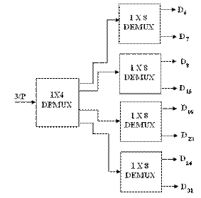
Q.51 You are given two types demultiplexers of four output and eight
outputs. Design a 32 output demultiplexer using these devices.
(4)
Ans:
Q.52 What
do you understand by a race around condition? (2)
Ans:
Race around condition: A race condition is said
to exist when in an asynchronous sequential circuit, two or more binary state
variables change value in response to a change in an input variable. When
unequal delays are encountered, the race condition may lead to an unpredictable
state for the state variables.
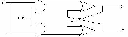
Q.53 Draw
the circuit diagram of master slave JK flipflop and explain its operation. (10)
Ans:
Master-Slave
JK Flip Flop:
This master- Slave consists of a J-K
Flip Flop as master & R-S Flip Flop as slave. Here when clock is positive,
the master may switch states and this information is held at its ends, but
isn’t propagated through to the slave. When the clock becomes negative, it
changes the slave while master is unaffected. Thus we can get negative edge
triggering. Also using this we can have transfer of binary content from one FF
to another and vice versa in the same clock pulse, because the information
doesn’t appear instantaneously at the end of the Master Slave Flip Flop.
Q.54 Draw
the diagram of a emitter coupled bipolar memory cell and explain its operation. (8)
Ans:
Bipolar
RAM cell is shown in the following figure:
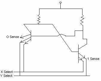
The sense, X select, Y select leads provide low resistance to
ground, grounding the emitters effectively and making the cell a flip flop.
When X and Y select lines are high, one of the sense leads is high and other is
low. This turns on one transistor and turns the other off. When X and Y are
turned low, the flip flop latches is that slate.
To read from the cell, both X select and Y select must
be high. In this condition both transistors are reverse biased and hence no
current flop in X and Y leads. The current in sense leads are measured and if
present represent logical 1. Thus if 0 sense has current and 1 sense has no
current, the flip flop is in state 0, that is the bit stores 0.
Q.55 Explain
the operation of PROM, and EPROM. (8)
Ans:
When production in small quantities is required a PROM or
programmable read only memory is used. When ordered PROM units contain all the
fuses intact giving all 1’s in the bits of stored words. The fuses in PROM are
blown using application of a high voltage pulse to the device through a special
pin. A blown fuse gives a binary ‘0’ state. This allows the user to program it
in the lab. Special programmes are used for this.
The hardware procedure for programming ROMs is irreversible &
once programmed the pattern is irreversible. The EPROM is erasable and can be
restructured. When EPROM is placed under special ultraviolet light for a given
period of time, the short wave radiations discharge the internal floating
gates. But individual bits can’t be reprogrammed as in case of EEPROM. The
programming takes lot of time, about 30 min and the whole ROM is reprogrammed.
The device has to be removed from its socket to reprogram it.
Q.56 Which are the important building
blocks in the architecture of the 741-type OPAMP? Comment on the function of
each block. (8)
Ans:
741 OPAMP circuit can be divided in various building blocks
·
BIAS CIRCUIT
·
SHORT – CIRCUT PROTECION CIRCUITRY
·
INPUT STAGE
·
SECOND STAGE
·
OUTPUT STAGE
BIAS CIRCUIT: The reference bias current,
IR is generated in the branch at the extreme left as shown in the
figure below, consisting of 2 diode–connected transistors Q11, Q12
and the resistance R5. Using a widlar current source formed by Q11,
Q12 and R4 bias current for first stage is
generated in collector of Q10. Another current mirror formed by Q8
and Q9 take part in biasing 1st stage.
·
The reference bias current IR is used
to provide proportional currents in collectors of Q13 (double
collector pnp transistor) which can be thought of two B-E junctions connected
in parallel. One output, collector of Q13B provides bias current for
Q17 and other output collector of Q13A provides bias
current for output stage of opamp.
SHORT-CIRCUIT PROTECTION CIRCUITRY: The
short circuit protection network consists of R6, R7, Q15,
Q21, Q24, R11, and Q22. If OPAMP output
is short circuited to any of the power supplies, one of the 2 output transistor
conduct a large amount of current. Such a large current can result in
sufficient heating to cause burnout of IC. To guard against this, output short
circuit, protection comes in picture. The function of this circuit is to limit
the current in the output transistors in event of a short circuit. Resistance R6
together with Q15 limits the current that would flow out of Q14
in the event of a short circuit. If current in emitter of Q14 exceed
20 mA, voltage drop across R6 exceeds 540mv, which turns Q15 on.
As Q15 turns on, its collector robs some of current supplied by Q13A
thus reducing base current of Q14. This limits the maximum current
that OPAMP can source to about 20 mA.
INPUT STAGE: The 741 circuit consists of
3 stages, input differential stage, intermediate single ended high gain stage
and output buffering stage. The input stage consists of transistors Q1 through
Q7, with biasing performed by Q8, Q9 and Q10.
The Q1 and Q2 act as emitter followers, causing the input
resistances to be high and delivering the differential input signal to the
differential common base amplifier formed by Q3 and Q4.
Transistors Q5, Q6, and Q7, and resistors R1,
R2 and R3 form the load circuit of the input stage. This
is a current mirror load circuit. The output of input stage is taken single
ended at collector of Q6. The use of lateral pnp transistors Q3
and Q4 in the first stage results in an added advantage of
protection of input stage transistors Q1 and Q2 against
B-E junction breakdown.
SECOND STAGE: This stage consists of Q16,
Q17, and Q13B and resistors R8 and R9.
Q16, act as an emitter follower, thus giving second stage high input
resistance. This minimizes the loading on the input stage and avoids loss of
gain. Q17 acts as common emitter amplifier with 100Ω resistor
in emitter. Its load is composed of the high output resistance of pnp current
source Q13 in parallel with input resistance of output stage. Using
transistor current source as a load resistance enables one to obtain high gain
without restoring to the use of large load resistances, which would occupy
large chip area and large power supply voltages. The output of second stage is
taken at the collector of Q17. Capacitor Ce is connected
in the feedback path of second stage to provide frequency compensation using
miller compensation technique.
OUTPUT STAGE: The purpose of output
stage is to provide the amplifier the low output resistance. Also O/P stage
should be able to supply large load currents without dissipating an unduly
large power in IC 741 uses an efficient output circuit known as class AB output
stage. The power dissipated in out put stage can be reduced by arranging for
the transistor to turn on only when an input signal is applied. One needs two
transistors, an npn to source output current and pnp to sink output current.
Both transistors will be cut off when VI =0, so the transistors are
biased as zero current. When VI goes + ve, QN conducts
while QP will be off. Reverse is also true. The class B circuit
stated above causes output signal distortion because of the fact that for VI
less than about 0.5 v, neither of transistors conducts and Vo= 0.
This distortion is known as cross over distortion. The output stage of 741
consist of complementary pair Q14 and Q20 .Where Q20
is a substrate pnp, transistors Q18 and Q19 are fed
by current source Q13A and bias the output transistors Q14 and
Q20. Q23 act as an emitter follower thus minimizing the
loading affect of the output stage on second stage.
Q.57 Define
the following for an OPAMP
(i)
Input bias current (ii) Input offset voltage
Briefly describe how the input
offset voltage can be measured. (6)
Ans:
INPUT BIAS CURRENTS:
Input Bias currents are due to dc imperfections. In order for OPAMP
to operate, its two input terminals have to be supplied with dc currents,
termed the input bias currents. These are shown in fig as IB1 and IB2.
It should be remembered that input bias currents are independent of the fact
that a real OPAMP has finite though large input resistances.
Average IB = 
And input offset current = |IB1-IB2|
INPUT OFFSET VOLTAGE –Since opamps are
direct coupled devices with large gains at dc, they are prone to dc problems.
If 2 input terminals of opamp are tied together to ground, it is found that a
finite dc voltage exists at output. The OPAMP can be brought back ideal value
of 0V by connecting voltage source of appropriate polarity and magnitude b/w input
terminals of input. This external sources balances input offset voltage of
OPAMP so Input offset voltage (VOS) must be of equal magnitude and
of opposite polarity to voltage applied externally.
Q.58 Write
a note on a ROM with an illustration. (9)
Ans:
A ROM is a device which consists of a decoder and a number of OR
gates so as to implement non-volatile permanent memory. The outputs from the
decoder are connected to the OR Gates in a pre-defined Fashion so that a
certain input results in a specific output, with the input acting as
addressing, we can emulate memory storage.
Modern ROMs are IC packages consisting of ‘n’ input lines and ‘m’
output lines. The various possible combinations of the input are the data, it
is called a ‘word’.
For ‘n’ input Line 2n addresses are possible for ‘m’
output Lines, each word consists of ‘m’ bits.
Internally, the ROM is a combinational circuit with AND gates
connected as a decoder and a number of OR gates for the outputs.
Consider a 32× 4 bits = 128 bits each word is 4 bits long and there
are 32 words. Also 32 = 25 hence there are 5 input Lines. Since each
word is 4 bits, there are 4 output lines. The block diagram is as follows. Also
shown is the internal logic of 32 x 4 ROM.
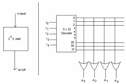
Internal logic of 32 x 4 bits ROM
Here, there are 128 fuses connecting the 32 outputs to each OR Gate
the fuses may be blown or set to obtain the correct output for each address.
Infect this flexibility lends to the fact that ROMS have numerous applications
including as function generators, number or data charts, as ROM in computers to
have the BIOS and much more.
Q.59 What
are the advantages of an active filter? Draw the circuit of a second order
Low-pass active filter and explain its functioning. (11)
Ans:
Advantages of Active Filters over passive filters:
·
Active realization provides considerably more
versatility.
·
Gain can be set to a desired value.
·
Transfer function can be adjusted without
affecting others.
·
Output impedance of the active circuit is also
very low, making cascading easily.
Active 2nd order Low Pass Filter circuits:
To analyze this consider
Zin =  =
=
 Leq =
Leq = 
LCR resonator

For LPF z and y are tied to ground and input voltage
is given at x.
wo = 
Q = wo C6R6 = 
Generally C4 = C6 = C and R1=
R2 = R3 = R5 = R
wo = 
Q = R6/R.
T(S) of LPF= 

Z6 = 
Vo = KVR

Q.60 What
are NMOS and PMOS logic circuits? Write the circuit of an NMOS nor-gate and
briefly explain. (7)
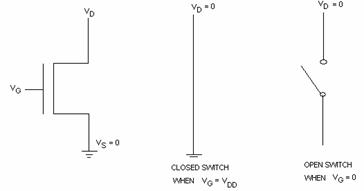
Ans:
Logic circuits are built with transistors. A transistor operates as
a simple switch. Shown below is a switch controlled by a logic signal x. When x
is low, the switch is open, and when x is high the switch is close.

Metal oxide semiconductor Field effect transistor (MOSFET) is one of
the most popular type transistors to implement a simple switch. There are two
different type of MOSFET’s known as NMOS and PMOS. These transistors have three
terminals: gate source and drain. Gate terminal is used as control terminal.
Symbol for NMOS
Symbol for PMOS
In NMOS when gate voltage is low there is no connection between
drain and source and transistor is turned off and acts as open switch. If VG
is high then transistor is turned on and behaves as a closed switch. PMOS
transistor has opposite behaviour of NMOS. These switches are used in logic
circuits to implement digital logic.


NMOS LOGIC
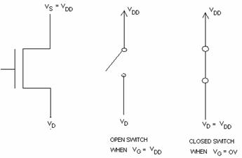
PMOS LOGIC
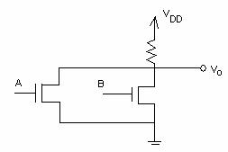
NMOS NOR GATE
Truth Table
 A B Vo
0 0 1
0 1 0
1 0 0
1 1 0
Here if either A or B or both are high, i.e. the gate voltage of the
transistor is high, then respective transistor would conduct and therefore Vo
will be close to zero. If both A and B are low then none of the two
transistors conduct therefore Vo will be pulled upto VDD
(high).
Q.61 Explain how a transistor can be used as a switch to connect and
disconnect a load  from
the source VCC. (8)
from
the source VCC. (8)
Ans:
Transistor as a switch to connect and disconnect a load RL from
the source VCC
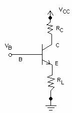
Explanation:
·
When a high voltage is aplied at the base (that
is ≈5v) the following conditions prevail at the 2 junctions
CB junction
VB= 5V
VC= 5-ICRC
VBC= ICRC
If RC is so chosen that Icsat RC
> 0.7V, the CB junction is forward biased
EB junction
VB = 5V
VE = IE × RL
VBE = 5-IERL
IF RL < 
BEjn  for ward bias
Thus, the transistor is in saturation and acts as a closed switch.
·
When a low voltage is applied at the base
(≈0V), the following conditions prevail
CB junction
VB = 0V
VC =5-ICRC > 0
VBC < 0 → CBjn reverse based
EB junction
VB=0V
VE= IERL
VBE < 0 →EBjn reverse biased
Thus the transistor is in cut off and it acts as an open switch.
Q.62 What
is the advantage of using Schottky transistors in a TTL gate with totempole
output? Draw the circuit of a 2-input Schottky TTL gate and explain its
features? (12)
Ans:
A reduction in storage time results in a reduction of propagation
delay. This is because the time needed to come out of saturation delays the
switching of the transistor. Saturation can be eliminated by using schottky
transistor. Its use decreases propagation delay without sacrifice of power
dissipation which would otherwise have happened if totempole output was used.

The diodes in each input shown in the circuit help clamp any ringing
that may occur in the input lines. Under transient switching conditions, signal
lines appear inductive, these cause signals to ring. The transistor ‘Q6’
and the resistors reduce the turnoff current spikes. The combination of
transistor ‘Q4’ & ‘Q5’ forms a Darlington pair. There
is no diode as in totem pole circuit. The new combination of ‘Q5’
& ‘Q4’ still gives 2’ VBE drops necessary to
prevent ‘Q4’ from conducting when output is low.
Q.63 What are the advantages and disadvantages of ECL? (4)
Ans:
The advantages of ECL are as follows:
a) It is the fastest of logic families as the
transistors do not enter saturation.
b) The propagation delays are as low as 1-2ns.
c) As a differential stage is used so common mode
signals are rejected.
d) High fan out is possible because of high input
impedance of differential amplifier and low output impedance of emitter
follower.
Disadvantages:
a) The power dissipation of 25 mW is quite high and
the noise margin of 0.3V is not very good
b) The voltage levels of -0.8V and 8 -1.8 v are not
compatible with other logic families.
c) External wires act as transmission lines due to
very high speed of signals.
Q.64 What is a full adder? Write the schematic and truth table of a full
adder. Describe how a full adder can be implemented using EX-OR/OR/AND gates.
(11)
Ans:
A full adder is an arithmetic circuit used for the addition of 2
bits which takes into account any carry from previous addition of lower
significant bits.
Truth Table
 A B Cin S Cout
0 0 0 0 0
0 0 1 0 0
0 1 0 1 0
0 1 1 0 1
1 0 0 1 0
1 0 1 0 1
1 1 0 0 1
1 1 1 1 1

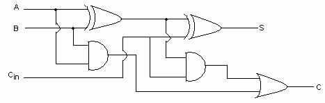
FULL ADDER
Q.65 What
do you mean by a data selector? Draw the logic circuit for a two-input
multiplexer using basic gates and briefly explain its operation. (5)
Ans:
Multiplexer is a device, which is used to select the data. We can
also call this Data Selector.
Multiplexer has 2n inputs, n selection lines and a single
output line. The output is selected depending on selection lines. If we want to
design a 2x1 multiplexor then input lines will be 2,output lines will be 1 and
single selection line.
Operation:-if S = 0, then output will be
A
S = 1, then output will be B
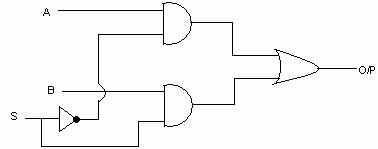
Logic circuit for 2 input multiplier
using basic gates
Q.66 What
is an ADC? Draw the schematic of an ADC that uses a binary counter and explain
its operation. (10)
Ans:
A counter based ADC uses a simple binary counter. The digital output
signals are taken from this counter (‘n’ bit) where ‘n’ is the desired number
of bits. The output of counter is connected to a DAC. If clock is applied to
the counter, the output of DAC is a stair-case wave-form. This waveform is
exactly the reference voltage signal for the comparator. First the counter is
reset to all 0’s. Then, when a convert signal appears, the gate opens and
allows the pulses to the counter. The staircase wave form is produced by the
DAC. When the reference voltage exceeds the input analog voltage, the gate is
closed, the counter stops and conversion is complete. The number stored in the
counter is the digital equivalent of analog input voltage.
The counter based ADC provides a very good conversion method.
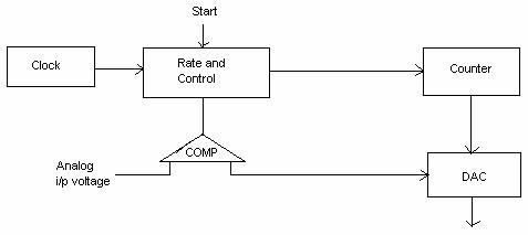
Counter Type ADC
Q.67 For the OPAMP circuit shown in the Fig.1, show that the output will
be proportional to the logarithm of the input voltage. (10)
Comment on the disadvantage of the circuit, if any.
Ans:
Log Amplifier :
Here a grounded base transistor is placed in a feedback path. Since
the collector is at virtual ground and the base is also at ground, the
transistor’s voltage current relationship becomes that of a diode and is given
by.
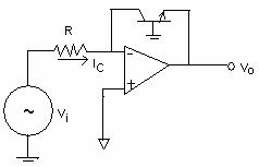

Since Ic =IE for a grounded base transistor.
Is=Tr saturation current = 10-13A
K=
Boltzmann’s constant
T
= absolute Temp in K. Therefore

Taking natural log on both sides we get
 Also
Also 
& VE =-Vo
Vo = -  Thus
Thus 
Q.68 What
is a flip-flop (FF)? What are the other names by which it is known? How many
outputs a flip-flop has and what are they called? What are the two types of
inputs does a clocked flip-flop have? (7)
Ans:
A flip-flop is a logic device used for storing a Single bit. It has
memory associated with it. It is also known as a clocked latch. A flip flop has
2 outputs.
One is the output and other is its complement. There are two inputs:
set and reset.
Q.69 What
is a shift register? With a neat schematic explain how J-K flip-flops can be
arranged to operate as a four-bit shift register. (9)
Ans:
Registers are data storage element in which
we can store more than 1 bit. They made up with flip-flop. Shift register can
shift data either in left or in right direction.
Initially we will reset all of the flip-flops. Then we can provide high
input to the flip-flop A, J1 & K1but there will be no
change output till we are not applying clock. Then clock will be at high
position and the output of the flip-flop will be high but there will be no
change in Flip-flop B. Now we will give 0 to the input J1 of
Flip-flop A and 1 to input K1 of the same flip-flop. This will reset
the flip-flop A and flip-flop B change to high. Similarly the process continues
the data will be serially shifted to the right direction
Q.70 How
are digital circuits employing MOSFETS categorised? Define each one of them
and mention their important features. How does CMOS internal circuitry differ
from N-MOS? (8)
Ans:
(a)
Digital circuits employing MOSFET’s are
categorized as :
A) NMOS B) PMOS C) CMOS
NMOS: The circuits employ n-channel
MOSFET’s. Its main features are:
– Power dissipation of about 0.1mw/gate at +5V VDD
– Propagation delay > 50ns.
- Fan-out – 10
PMOS: The circuits employ p-channel
MOSFET’s. Main features are:
- Power dissipation of about 0.1m w/gate
- Propagation delay > that of NMOS
- Fan out less than that of NMOS
- Package density less then that of NMOS
CMOS – The Circuits employ a combination
of NMOS and PMOS
- Power dissipation of about 0.01 mw/gate at +5 VVDD.
- Propagation delay < 50 ns
- Lower packaging density
- Very high for fan out -50
CMOS employs PMOS & NMOS transistors on the same chip while NMOS
chips use only NMOS transistors.
Q.71 What is meant by of the term RAM? What
is its meaning? How is it used in computers and what is its major
disadvantage? Distinguish
between a Static RAM and a Dynamic RAM. (8)
Ans:
A memory unit is a collection of storage cells together with
associated circuits needed to transfer information in and out of the device.
The time it takes to transfer information to or from any desired random
location is always same, hence the name RAM.
It is used for storing temporary data, as it is volatile. The
variables required for a particular program are stored. Here RAM can perform
both read and write operations. Therefore all the variables during the ALF are
stored here.
The static RAM (SRAM) consists of internal latches that store the
binary information. The stored information remains valid as long as power is
there.
The dynamic RAM stores information in the form of charges on
capacitor. The capacitors are provided inside the chip by MOS transistors. The
stored charge tends to get discharged with time and the charge has to be
periodically refreshed.
DRAM offers reduced power consumption and larger storage capacity in
a single memory chip. SRAM is easier to use and has shorter read and write
cycles.
Q.72 Draw
the circuit of a basic instrumentation amplifier that uses three OPAMPS.
(3)
Ans:
Instrumentation Amplifier with 3 OPAMPS
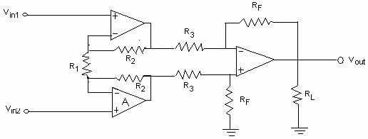
High gain (Differential)

Q.73 Which
is the feature of the commercially available OPAMPS that helps the designer to
design active filters upto frequencies of several megahertz. You are given a
Low-pass and a high-pass filter, how would you construct a band-reject filter?
What is the transformation to be used to convert a LPF to a HPF. (9)
Ans:
A Band-pass filter is formed by cascading a HPF and LPF section. If
we subtract the band pass filter output from its input we get band reject
filter. We get band reject filter.
The Band pass filter has an inverted output as the gain or transfer
function is negative. Therefore while implementing Fig(a) we must use a summer
instead of a subtractor. Also the band pass filter has a gain of A0
so that output at the centre frequency – A0 X Vi. To
completely subtract this output, the input of the summer must be precisely A0
Vi. Thus a gain of Av must be added between the
input signal and the summer as in fig(C). The output of the circuit in the
s-domain is


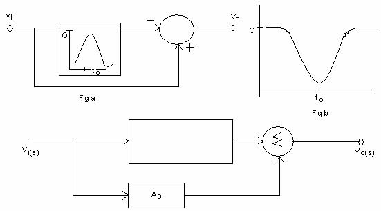

This is the transfer function for a second order notch filter.

LPF to HPF Transformation:
We get the high pass characteristics by the following low pass to
high pass transformation
p = 1/S. For example, a third order Butterworth low pass transfer
function in p-domain
is given as  can be transformed to high pass by the
transformation
can be transformed to high pass by the
transformation
p = 1/s as 
Q.74 What
are the advantages of switched capacitor filters? (4)
Ans:
In active RC filters the resistor values needed are generally much
too large for fabrication on a monolithic IC chip. Integrated resistors have
poor temperature and linearity characteristic.This is the major reason that
active filters have not been fully integrated in MOS technology.
In switched capacitor filter the RC products are set by capacitor
ratios and the switch period. In MOS technology the accuracy and the values of
these quantities are suitable for the implementation of selective filters. The
large resistor values required for active filters are easily simulated by the
combination of small value capacitors and MOS switching transistors. Thus a
filter of relatively high order becomes an integrated circuit of small size,
with low power consumption and high reliability.
Q.75 Define
the Chebyshev polynomial as power the recursive formula. Indicate the above
polynomial valid for the passband and stopband of a low-pass Chebyshev filter.
Briefly describe the properties of the Chebyshev polynomial.
(9)
Ans:
The chebyshev polynomial is defined as:

This can be expanded as follows:

The recursion formula for this polynomial can be written as:

For passband, 
For stopband, 

The properties of chebyshev polynomial can be shown as:
1)
These
functions are distorted cosine waves, bunched towards w = ±1
2)
Ripples
within the boxes in which the response is confined are always equal , ±1 for Cn
and between +1 & 0 for Cn2
3)
At
w=0,
Cn(0) = ±1 for n even
= 0 for n odd
Q.76 Write
a note on the basic CMOSFET switch. (7)
Ans:
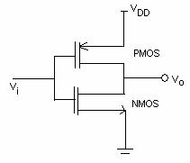
The above shown circuit can function as a CMOS switch. When Vi
< Vt the output voltage V0 will be equal to VDD.
Thus, switch will be open while when, Vi = VDD, the
output voltage V0 will be nearly 0V. Thus switch is closed. This is
so since in the former case PMOS will be conducting while in later case NMOS
will be conducting. Here static power dissipation is very less.
Q.77 Draw
the circuit of a 3-input open-collector TTL NAND gate and explain its
operation. (9)
Ans:
Open Collector TTL NAND Gate:These gates
are of multiple emitter type, three inputs A, B and C are connected to emitters
of Q1. These emitters behave like input diodes. Base – collector junction of Q1
also behaves as another diode. The output of the TTL gate is taken from the
open collector of Q3. If any of the I/P is low at 0.2V, the corresponding input
diode conducts current through Vcc.
Q.78 What
is the principle on which ECL operates? Based on this, what is the other name
given to ECL? Draw the circuit of a two-input ECL OR/NOR gate and briefly
explain. (7)
Ans:
ECL is recommended in high frequency applications where its speed is
superior.
Justification:
1.
It is not saturated logic, in the sense that
transistors are not allowed to go into saturation. So, storage time delays are
eliminated & therefore the speed of operation is increased.
2.
Currents are kept high, and the output impedance
is so low that circuit & stray capacitances can be quickly charged and
discharged.
3. The limited voltage swing that is the logic levels are chosen clock
to each other.
Important features:
1.
One advantage of differential input circuit in
ECL gates is that it provides common mode rejection – power supply noise common
to both sides of the differential configuration is effectively cancelled out.
2.
Also, since the ECL output is produced at an
emitter follower, the output impedance is desirably low. As a consequence, the
ECL gates not only have a larger fan out but also are relatively unaffected by
capacitive loads.
Q.79 What is an encoder? Draw the schematic of a general encoder with X
inputs. Explain briefly its operation. Give the logic circuit and truth table
for an octal-to-binary simple encoder with active-low inputs. (13)
Ans:
An
encoder is a device whose inputs are decimal digits and whose outputs are the
coded representations of those inputs. An encoder has a number of input lines
only one of which is activated a given time & produces an N bit output code
depending upon which input is activated.
General block diagram of an encoder with M Input and N output is as
shown below:-
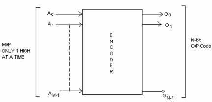
An octal to binary encoder (8 line to 3 line encoder) accepts 8 input
lines and produces a 3 bit output code corresponding to the activated input.
The following figure shows the truth table and logic circuit for an octal to
binary encoder with active low output.
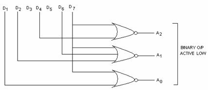
Logic Diagram
Truth table:
|
Octal digits
|
Binary
A2
A1 A0
|
|
D0
|
0
|
0
|
0
|
0
|
|
D1
|
1
|
0
|
0
|
1
|
|
D2
|
2
|
0
|
1
|
0
|
|
D3
|
3
|
0
|
1
|
1
|
|
D4
|
4
|
1
|
0
|
0
|
|
D5
|
5
|
1
|
0
|
1
|
|
D6
|
6
|
1
|
1
|
0
|
|
D7
|
7
|
1
|
1
|
1
|
Q.80 What
do you mean by a priority encoder? Can such a circuit be used to take care of
the draw-back of the simple circuit explained in Q79 above? (3)
Ans:
The encoder discussed in Q79 will work correctly only if one of the input
lines is high at any given time. In some practical systems, two or more decimal
inputs may inadvertently become high at the same time.
A priority encoder is a logic circuit that responds to just one input
in accordance with some priority system, among all those that may be
simultaneously high.
The most common priority system is based on the relative magnitudes
of the input; whichever decimal input is the largest, it will be encoded.
Such a circuit can be used to take care of the drawback of the
simple circuit as explained in Q79.
Q.81 What
circuit is commonly used to improve the stability of the conversion process in
an ADC? briefly explain its features. (10)
Ans:
A counter based ADC uses a simple binary counter. The digital output
signals are taken from this counter (‘n’ bit) where ‘n’ is the desired number
of bits. The output of counter is connected to a DAC. If clock is applied to
the counter, the output of DAC is a stair-case wave-form. This waveform is
exactly the reference voltage signal for the comparator. First the counter is
reset to all 0’s. Then, when a convert signal appears, the gate opens and
allows the pulses to the counter. The staircase wave form is produced by the
DAC. When the reference voltage exceeds the input analog voltage, the gate is
closed, the counter stops and conversion is complete. The number stored in the
counter is the digital equivalent of analog input voltage.
The counter based ADC provides a very good conversion method.
Q.82 What are the advantages and disadvantages of Dual-slope ADCs?
Comment on their major application. (6)
Ans:
Advantages of dual scope ADC’s:
Ø
Relatively
inexpensive because it does not require precision components like DAC or VCO.
Ø
Low
sensitivity to noise.
Ø
Low
sensitivity to the variations in component values caused by temporary changes.
Disadvantages:
Ø
Large
conversion time and thus it is not useful for data acquisition systems.
Ø
Restricted
to signals having low to medium frequencies.
Applications:
Ø
Digital
voltmeters and multimeters where slow conversion is not a problem.
Q.83 With
the help of a block schematic diagram and neat wave forms, explain a clocked
J-K flip-flop that is triggered by the positive – going edge of the clock
signal. (10)
Ans:
The JK flip-flop is
very versatile and most widely used having no invalid state like that of SR flip-
flop. J and K are the synchronous control input.
|
Inputs
|
Clock
C
|
Q
|
Comment
|
|
J K
|
|
0
|
0
|
  
|
Q0
|
No
change
|
|
0
|
1
|
|
0
|
reset
|
|
1
|
0
|
|
1
|
set
|
|
1
|
1
|
|
Q0
|
toggle
|
Q.84 What
is an asynchronous counter? Why is it so called? Based on its operation, it
is commonly referred to as what? What do you mean by ‘MOD Number’ as applied
to an asynchronous counter? (6)
Ans:
Asynchronous counters are the simplest type of counters, easiest to
design requiring minimum hardware. They are called so because all the flip
flops in the counter are not made to change their states simultaneously that is
these are not clocked simultaneously. An asynchronous counter uses T flip flops
to perform the counting function.
They are commonly called as ‘Ripple counters’ because only one of
the flip flops is directly clocked from an external clocks source and as the
number of pulses increases, the consecutive flip flops get clocked which gives
a ‘ripple effect’.
The “modulus” of a counter refers to the total number of distinct
state (including zero) that the counter can store.
Q.85 What
is the type of MOSFET used in CMOS logic family? Mention the advantages and
disadvantages of CMOS. With a neat sketch for illustration, briefly describe
the basic CMOS NOR gate. (10)
Ans:
The CMOS logic family uses both P&N channel MOSFETs in the same
circuit to realize several advantages over PMOS & NMOS families.
Advantages and disadvantages:
Ø
Faster
than other MOS families.
Ø
Consumes
less power as compared to other MOS families.
Ø
Can
be operated at higher voltages resulting in improved noise immunity.
2 Input MOS NOR Gate
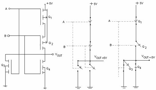
(a)
(b) (c)
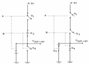
(d)
(e)
|
|
A
|
B
|
Q1
|
Q2
|
Q3
|
Q4
|
Vout
|
|
(b)
|
0V
|
0V
|
ON
|
ON
|
OFF
|
OFF
|
5V
|
|
(c)
|
0V
|
5V
|
ON
|
OFF
|
ON
|
OFF
|
0V
|
|
(d)
|
5V
|
0V
|
OFF
|
ON
|
OFF
|
ON
|
0V
|
|
(e)
|
5V
|
5V
|
OFF
|
OFF
|
ON
|
ON
|
0V
|
Truth Table
Q.86 How does a static RAM cell differ from a dynamic RAM cell? What are
the main drawbacks of dynamic RAM compared to a static RAM? List the
advantages of dynamic RAM compared with static RAM. (6)
Ans:
Static RAM cells are essentially flip flops that will stay in a
given state indefinitely, provided that power to circuit is not interrupted. On
the other hand, dynamic RAMs store data as changes on capacitors. With DRAMs,
the stored data will gradually disappear because of capacitor discharge;
therefore, it is necessary to periodically refresh the data (that is recharge
the capacitors).
|
|
SRAM
|
DRAM
|
|
1.
|
The are available in both bipolar and MOS
technologies.
|
They are fabricated only using MOS technology.
|
|
2.
|
Low capacity
|
High capacity due to simple cell structure.
|
|
3.
|
High power requirement
|
Low power requirement
|
|
4.
|
High speed
|
Moderator
speed
|
|
5.
|
More costly
|
Less costly
|
|
6.
|
Used
where small size of memory required and high speed is desirable.
Ex:
H Processor controlled equipments; H controllers
|
Used where
high capacity & low power dissipation are required. Ex: Internal
memory (main) of most PCs is DRAM.
|
|
7.
|
No data refreshing is required.
|
Data
refreshing is required.
|
Q.87 What
is an OPAMP? What do you mean by common mode operation? What will be the
output voltage for the above operation, ideally? (4)
Ans:
OPAMP (Operational Amplifiers) are ideal voltage amplifiers which
are characterized by OPAMP equation
V0
= A (V+ - V-), where A is the gain.
As its name suggests it can do various ‘operations’ such as
addition, subtraction, etc.
Common Mode Operation:-
Common Mode Operation means that the same voltage is applied at the
positive and negative inputs of the OPAMP.
The output of the OPAMP should ideally be zero in common mode
operation.
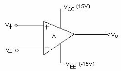
Q.88 Briefly
explain how the following can be measured for an OPAMP:
(i)
Input offset voltage  (ii) Bias current
(iii) Input offset current  (9)
(9)
Ans:
(i)
Input offset voltage (Vi0): It is
the voltage that must be applied between the two input terminals of an OPAMP to
null the output. Vio could be positive or negative

(ii)
Bias
Current (IB): It is the average of the current that flows into the
inverting and non-inverting input terminals. Bias current at one input is
forced to flow through a large resistor. Since the bias current at the other
input does not flow through a resistor, it produces no voltage and has no effect
on the output voltage.

By selecting a large resistance, bias current can be measured.
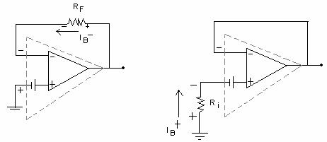

(iii)
Input offset current (Ii0):- Once
IB+ & IB- are measured, Ii0
can be calculated as
Ii0
= IB+ - IB-
Q.89 What is the advantage of Schottky diode over an ordinary PN-junction
diode in terms of speed of operation? Support your answer with relevant
comments. (4)
Ans:
The schottky–barrier diode is formed by bringing metal into contact
with a moderately doped n-type semiconductor material. The resulting metal
semiconductor junction behaves like a diode conducting current in one direction
from metal anode to semiconductor cathode and acting as an open-circuit in
other direction.
The speed of operation of schottky diode is faster as compared to
ordinary PN junction diode as in this diode current is conducted by majority carries
(electrons). Thus this does not exhibit the minority carrier charge storage efforts
formed in forward biased pn junction As a result it can be switched from on to
off and vice versa much faster than is possible with pn-junction diodes.
Q.90 What
is an active filter? Define an ideal band-pass filter and illustrate its
response characteristic. Can active filters be designed up to frequencies of
several MHz? Justify your answer. (6)
Ans:
Active Filters are realized using components. Since simulation of L
using OPAMP’s is much simpler and easier than using inductor itself. So Active
Filters have advantages over passive filters. Other advantages of Active
Filters over passive filters are as follows:
·
Active
realization provides considerably more versatility.
·
Gain
can be set to a desired value.
·
Transfer
function can be adjusted without affecting others.
·
Output
impedance of the active circuit is also very low, making cascading easy.
IDEAL
BANDPASS FILTER
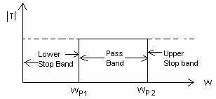
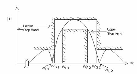
1.
The
pass band edge = wp1, wp2
2.
Maximum
allowed variation in passband transition Amax
3.
The
stopband edge = ws1 , ws2
4.
Minimum
required stopband attenuation is Amin
Q.91 Starting
from fundamentals, explain the meaning of the term “SWITCHING TIME” as applied
to a semiconductor diode. What is the use of the above quantity?
(8)
Ans:
Switching Time of Diode :
When the bias voltage of a forward biased diode is switched abruptly
to a negative voltage, the diode current does not reverse instantaneously.
5.
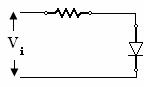
For t < 0, the constant forward bias causes the a steady forward
current, If = (Vf – VD)/R. With a steady reverse
voltage applied for t >0, we expect the minority carrier profile to change.
This changeover requires (i) the diffusion capacitance, which is dominant
during forward bias, is fully discharged (ii) the depletion region is widened
and depletion region is charged in the opposite direction. The two capacitances
involved in the sequence cause the time delays ts and tt
as shown in figure (b) where ts is the storage time and tt
is the transition time.
The storage time ts is the time taken by the diffusion
capacitance to discharge.The transition time , tt is the time taken
by the depletion capacitance to charge to the applied reverse voltage. The sum
of ts and tt is the reverse recovery time, trr,
which is the turn-off delay of the diode. Thus at higher forward current since
more charge is stored, longer storage time ts is needed to discharge
the diffusion capacitance.
The forward
recovery time, tfr is the time delay of the diode in switching from
off state to on
state.
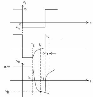
Q.92 Briefly
explain how a transistor can be used as a switch. (7)
Ans:
A BJT is used in cut off and saturation mode when it is used as a
switch.
When Vi < 0.5V, the transistor is in cut off mode. Thus , iB
= iC = 0 and V0 = VCC=VCE. This
corresponds to an open switch condition.
As input voltage Vi is increased, the transistor enters into active region
and iC=βiB. Now the output voltage V0 is
given by  .
Thus as iC increases, V0 decreases correspondingly. When
VCE≤0.2V, then transistor enters into saturation and device
becomes on resulting in closed switch.
.
Thus as iC increases, V0 decreases correspondingly. When
VCE≤0.2V, then transistor enters into saturation and device
becomes on resulting in closed switch.
Q.93 Write
a note on switching speed of BJT. (4)
Ans:
The speed at which a BJT can change its logic states is limited by
the delays of the transistor in switching between saturation and cut off modes
of operation. When the transistor is operating in the cut off mode, the emitter
base junction is 0 or reverse bias. As input voltage changes in forward
direction, base current decreases. The collector current however does not attain
its saturation values instantaneously. Because the emitter base junction
transition capacitance must be charged to forward bias voltage. As the EBJ
becomes forward biased, the junction capacitance becomes predominantly
diffusion capacitance which controls the collector current. This contributes to
the delay time td. Once the transistor is brought from cut off to
active mode, the collector current begins to increase. Now the forward bias
diffusion capacitance at EBJ charges exponentially while Ic rises as
βIB and reaches
its maximum of Icsat. The time taken in reaching Icsat is
tr. The sum of delay and rise time is the turn on delay of BJT. The
delay in turn off process of the transistor is caused primarily by the removal
of the excess minority carriers in the base region. When input voltage switches
from VH to VL, the collector current continues at its
saturation level until the excess charge is removed from the base region. The
storage or saturation delay is the interval during which Ic remains
at Icsat. The fall time of the collector current during which
transistor goes from active to cut off mode, is called tf. The sum
of storage and fall time is turn off delay.
Q.94 What is the problem faced by switched capacitor filters and what is
normally done in practice to avoid the same? Explain the working of a switched
capacitor cell. (5)
Ans:
In active RC filters the resistor value needed are generally much
too large for fabrication on a monolithic IC chip. Integrated resistors have
poor temperature and linear characteristic .This is the major reason that
active filters have not been fully integrated in MOS technology.
In switched capacitor filter the RC products are set by capacitor
ratios and the switch period. In MOS technology, the accuracy and the values of
these quantities are suitable for the implementation of selective filters. The
large resistor values required for active filters are easily simulated by the
combination of small value capacitors and MOS switching transistors. Thus a
filter of relatively high order becomes an integrated circuit of small size,
with low power consumption and high reliability.
The only drawback of these filters is that these are noisier as
compared to the active filters.
Switched
Capacitor cell:
In switched
capacitor filter, the large resistor values required are simulated by the
combination of small value capacitors (e.g. 10pf) and MOS switching
transistors.
Considering the
switched capacitor network shown below we see that when switch S is initially
in position ‘a’ the capacitor C is charged to voltage V1. The switch
is then thrown to position ‘b’. The capacitor C is discharged to the voltage V2
assuming V2<V1. The amount of charge that flows
through the capacitor C is thus,
Q = C (V1-V2)
If switch is
thrown back and forth every TCK second, then the current i that
flows through the capacitor C is equal to the rate at which the charge is
transferred through the circuit via C and is given by
Thus the size of
an equivalent resistor R which would perform the same function as this circuit
is given by
ф and ф’ are out of phase
clock signals
|
|
Q.95 What
is an ADC? Compare the performance of a flash ADC with that of a Dual Slope
ADC. (7)
Ans:
The process of converting an analog voltage into corresponding
digital signal is known as analog to digital conversion. It is accomplished by
using an analog to digital convertor (ADC)
Different types of ADCs are as under:-
1.
Counter
type ADC
2.
Flash
type ADC
3.
Dual
slope type ADC
4.
Successive
approximation type ADC
|
|
Flash type
ADC
|
Dual Slope
type ADC
|
|
1
|
Flash type ADC
is the fastest ADC with a conversion time of 10 to 50 ns.
|
Dual slope
type ADC is the slowest ADC with very high conversion times.
|
|
2
|
About 2n
– 1 comparators are required to convert t a digital signal having ‘n’ bits.
Besides this a priority encoder is required. This adds to the cost.
|
This ADC is
least expensive requiring just 2 comparators ,counter etc.
|
|
3
|
This ADC fails
if the output required has 3 or 4 bits as the system becomes expensive.
|
This ADC can
be used for high order bit outputs.
|
|
4
|
Flash A/D conversion
techniques enable these IC’s to be used in many high speed data acquisition
such as TV video digitising, radar analysis, medical ultrasound, imaging, etc
|
Dual slope
conversion techniques having high conversion time are used in digital
voltmeters and other low frequency applications.
|
Q.96 With neat sketches for
illustration, explain the operation of the circuit shown in Fig.2, by taking
the voltage  as
a sinosoidal signal and
as
a sinosoidal signal and  equal to zero. (7)
Fig 2
Ans:
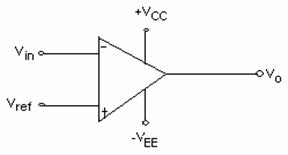
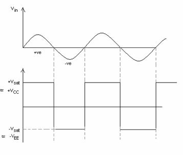
When the sinusoidal input is > 0, the output saturates to +Vcc
and when it is <0, the output saturates to – Vee. The circuit
assumes no delay in switching from –Vee to +Vcc and vice
versa. In practice, there is a finite time taken by the system to rise from –Vee
to +Vcc which is characterised by the slew rate of the OPAMP.
Q.97 What
do you mean by ‘acquisition time’ as applied to a sample-and-hold circuit? (2)
Ans:
Acquisition time refers to the time
interval between the change in analog signal at the input and appearance of
equivalent digital value at the output of the ADC.
The acquisition time is the sum of
a. Sample time – time taken to
sample the signal
b. Hold time – time during which
digital conversion takes place.
Q.98 Write the circuit of an antilog
amplifier that uses two OPAMPS and derive the equation for the output voltage
from the circuit. (10)
Ans:
Antilog amplifier
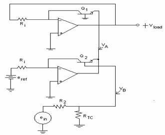
From the figure above
Since the base of Q1 is tied to ground , therefore
VB is the base voltage of Q2 and is output
from the R2, RTC voltage divider.
The voltage at the emitter of Q2 is
On substitution, we get
But the emitter of Q2 is VA thus

Where
Q.99 When
do you use NMOS logic circuits? Write a brief note on CMOS logic. (6)
Ans:
NMOS logic circuits are used when:
a.
Density
has to be increased as NMOS transistors can be fabricated in less area than bipolar
transistor.
b.
NMOS
transistors can be used as variable resistors as well.
c.
NMOS
circuits have dissipation of less than 0.1 mw per gate but have slow speeds of
about 50 ns. So when low power dissipation is the primary objective there NMOS
circuits are used.
d.
NMOS
circuits also have higher fan– out of about 50.
e.
As
NMOS circuits are faster than PMOS and also require less area than PMOS. So,
they are preferred to PMOS.
CMOS or complimentary MOS circuits take advantage from the fact that
both n-channel and p-channel devices can be fabricated on the same substrate.
They consist of both kind of MOS devices interconnected to form logic functions.
The basic circuit is the inverter.
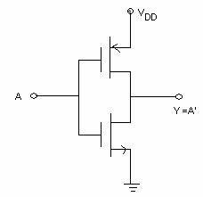
MOS transistors act as electronic switches. When CMOS logic is in a
static state, its power dissipation is very low. This is because there is
always an off transistor in the path. The static power dissipation is about
0.01 mW. Moreover at high frequencies, the power dissipation increases to about
1 mW.
CMOS logic is usually specified for a single power supply operation
over a voltage range of 3 to 18 V with typical VDD values of 5V. The
propagation delay with +5V VDD ranges from 5 to 20 ns depending on
the type used. The fan-out is usually 30 when operated at 1MHz and decreases
with increase in frequency. The noise margin is usually 40% of power supply
voltage.
The CMOS fabrication is simpler than TTL and provides greater
packing density.
Q.100 Which are the
saturated bipolar logic families of interest? Write the circuit of an unloaded
BJT inverter and explain briefly its transfer characteristics. (12)
Ans:
The saturated bipolar logic families are in which gates are realized
using the saturation and cut off modes of bipolar transistors. The three basic
bipolar logic families of interest are:
a.
RTL – Resistor Transistor logic
b.
DTL – Diode Transistor logic
c.
TTL – Transistor Transistor logic.
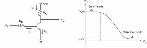
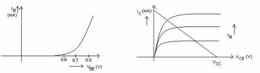
Input Characteristic Output
Characteristic
The base emitter graphical characteristic shows a plot of IB
versus VBE. If the base emitter voltage is less than 0.6V, the
transistor is said to be cut off and no base current flows. When the VBE
> 0.6V the transistor conducts and IB starts rising very fast
while VBE changes very little. When VBE is less than
0.6V, the transistor is cut off with IB = 0 and negligible current
flows in collector. In the active region VCE can be anywhere between
‘0.8V’ and VCC and IC= βIB. It must be realized that ‘IB’ may be
increased to any value, but ‘IC’ is limited by external circuit characteristics.
As a result a situation is reached where βIB > IC. In this condition the transistor
is in saturation. ‘VCE’ is about ‘0.2V’ when transistor is in
saturation region.
Q.101 Which are the
factors that determine the operating speed of a logic gate? How can the speed
performance of a TTL be improved? (4)
Ans:
The factors that determine the operating speed of a logic gate are:
i.
Storage
time –
when a transistor switches its state from saturation to cut off, a particular
time interval is required for this process. Reducing storage time reduces
propagation delay.
ii.
RC
time constants
– reducing RC time constant by reducing the resistor values reduces the
propagation delays but increases the power dissipation.
The speed of TTL gates can be increased by the either reducing the
storage time by using schottky diodes or preventing transistor from going into
saturation or by reducing ‘RC’ time constants.
Q.102 How do you
compare a PAL device with the PLA? Illustrate the structure of a simple
four-input, three-output PAL device and mention its features. Explain how the
PAL device can be used to realise the two Boolean functions given below:
 . (10)
Ans:
PAL or programmable array logic is a device with a fixed OR array
and programmable AND array while PLA is a logic device just like PROM but it
has both OR and AND array programmable.
In PAL as only AND gates are programmable so it is easier to
program, but is not as flexible as PLA.
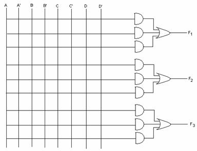
The above diagram shows a 4 input 3 output PAL device. The AND array
with crosses is shown programmable while OR gates are hard wired. Unlike the
PLA, the product term can’t be shared among 2 or more OR gates.


The above can be implemented using 3 input, 2 output PAL device with
4 wide AND-OR structure.
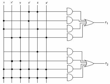
The above PAL shows the implementation of the desired function.
Q.103 Describe the
realisation of the Boolean function,  using an 8-to-1 line multiplexer. (6)
Ans:
The boolean function  can be realized using 8 to 1
multiplexer by
can be realized using 8 to 1
multiplexer by

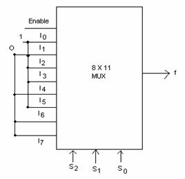
Q.104 Distinguish
between a PROM and an EPROM. What are their disadvantages? (8)
Ans:
When production in small quantities is required a PROM or
programmable read only memory is used. When ordered PROM units contain all the
fuses intact giving all 1’s in the bits of stored words. The fuses in PROM are
blown using application of a high voltage pulse to the device through a special
pin. A blown fuse gives a binary ‘0’ state. This allows the user to program it
in the lab. Special programmes are used for this.
The hardware procedure for programming ROMs is irreversible &
once programmed the pattern is irreversible. The EPROM is erasable and can be
restructured. When EPROM is placed under special ultraviolet light for a given
period of time, the short wave radiations discharge the internal floating
gates. But individual bits can’t be reprogrammed as in case of EEPROM. The
programming takes lot of time, about 30 min and the whole ROM is reprogrammed.
The device has to be removed from its socket to reprogram it.
Q.105 What do you
mean by “MOD- number” of a counter? Write the step-by-step procedure to
construct any MOD-N ripple counter, where N is less than  , with ‘n’ denoting the number
of flip-flops. (8)
, with ‘n’ denoting the number
of flip-flops. (8)
Ans:
If a counter is MOD-N counter it means that it will count total N
states in a packet in sequence. For example a MOD-3 counter can count from 0 to
2 (i.e. 00, 01, 10) or 9 to 11 (i.e. 1001, 1010, 1011). In general, a Mod-N
counter counts from 0 to N-1 states.
Following are the steps to construct a MOD-N ripple counter.
(N < 2n) where n = No. of flip flop’s
1)
For
MOD-N (N < 2n) counter, first we take n complementing flip
flop’s [e.g. for MOD-5 counter we take
3 JK or T flip flop’s]
2)
In
T flip flop we connect all the inputs
to high & in JK flip flop we connect
both J and K at high.
3)
The
flip flop at the least significant
position is connected to count pulse as a clock (inverted).
4)
Next
significant positions clock pulse is connected to the output of the least
significant position (inverted).
5)
In
the similar fashion the clock of every flip
flop is connected to the output of
its lower significant state inverted. In this way an MOD-N when N = 2n
counter (ripple) is constructed.
6)
However
for N < 2n, we observe the first state to the skipped (e.g. in
MOD-5, it is 101, it should count 0 to 4 and then again come to 0. We take high
inputs and connect these to a NAND gate. When this stage comes for a fraction, the
NAND gate will give low output. The output of NAND gate is connected to all
clear inputs of all flip flop’s. Thus immediately after 4 it will come to zero.
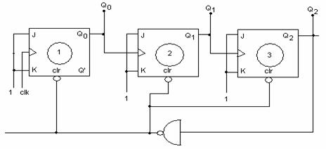
MOD – 5 ripple counter
Q.106 What is it
that an OPAMP contains to achieve a very high voltage gain? What do you mean
by common-mode rejection as applied to an OPAMP? (4)
Ans:
The operational amplifier consists of four cascaded blocks. The
first two stages are cascaded differential amplifiers; third stage is level
shifter and forth is output driver.
It is the differential amplifier which provides high gain and high
input resistance. It amplifies only to difference mode signals and rejects to
common mode signals.
If a common signal is applied to both the inputs of an OPAMP and
output is taken differentially, then the output voltage will be zero. Thus we
say that OPAMP does not respond to common mode signal or it rejects common mode
signal.
The relative sensitivity of an OPAMP to a difference signal as
compared to a common – mode signal is called common-mode rejection ratio.
Q.107 With a circuit
for illustration, explain the effect of the input offset voltage for the OPAMP,
 (which is
normally specified in the manufacturer’s data sheet) on the output. (7)
(which is
normally specified in the manufacturer’s data sheet) on the output. (7)
Ans:
Due to unavoidable imbalances inside the practical OPAMP, it may be
possible that the output voltage is not zero with zero input voltage. Therefore
we may require to apply a small voltage at the input terminal to make output
voltage zero. This input voltage is called input offset voltage (Vio).
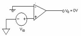 input offset voltage
Effect of Vio on
the output:
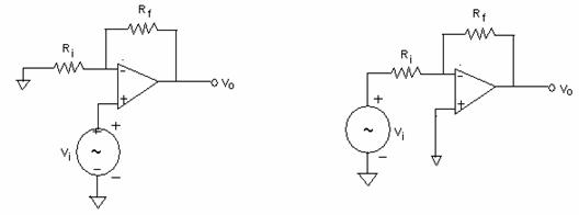
Fig (a) non-inverting
amplifier Fig (b) inverting amplifier
if Vi is set to zero the circuits of Fig
(a) & (b) become same as in Fig (c).
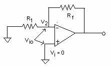

The voltage V2 at negative input
terminal is given by

Thus the output offset voltage of an OPAMP in closed loop
configuration is given by equation (3)
Q.108 Write a note
on frequency response of OPAMPS. (5)
Ans:
Ideally, an OPAMP should have an infinite bandwidth. The practical
OPAMP gain, however, rolls off at higher frequencies. This roll off in the gain
is due to capacitive components in the equivalent circuit of OPAMP. This
capacitance is due to the physical characteristics of the device used and
internal construction of OPAMP. For an OPAMP with only one corner frequency,
all the capacitor effects can be represented by single capacitor.
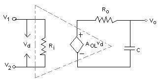
High frequency model of an OPAMP with single
corner frequency
The
open loop voltage gain of an OPAMP with only one corner frequency is

Or

Or

Where f1 = is the corner frequency
There is one pole due to RoC and therefore
one -20 db/decade roll off comes into effect.
Frequency
response with one corner frequency
A practical OPAMP, however, has number of stages and each stage
produces a capacitive component. Thus there will be a number of different break
frequencies.
Q.109 What is the
role of an OPAMP in an active filter? Define an ideal low-pass filter. Write
the equation for the squared magnitude response of a low-pass Butterworth
filter. Mention the variables involved in the above equation.
(7)
Ans:
Filter is a frequency selective circuit that passes signals of
specified band of frequencies and attentuates the signal of frequencies outside
the band. For low frequency application passive filters can not be used as
inductors become large, heavy and expensive and result is high power
dissipation.
The active filters overcome the abovementioned problems of the
passive filters.
These use OPAMP as the active element; resistors and capacitors as
the passive elements. The active filters, by enclosing a capacitor in the feed
back loop, avoid using inductors. OPAMP is used in non inverting configuration,
it offers high input impedance and low output impedance. This improves the load
drive capacity and load is isolated from the frequency determining network.
Ideal low pass filter: An ideal low pass
filter transmits frequencies uptill wp With unity magnitude of
transmission which is called as filter pass band and frequencies beyond wp
are transmitted with zero magnitude of transmission, called as filter stop band
wp is called as pass band edge.
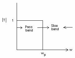
Idealized
characteristic of a low pass filter
This
idealized characteristic is also known as brick wall type response.
The magnitude function for an nth order Butterworth filter with a
pass band edge wp is given by

At w=wp 
The
parameter  determines
the maximum allowed variation in pass band transmission, Amax,
according to
determines
the maximum allowed variation in pass band transmission, Amax,
according to
Amax = 20 log 
N is the order of filter, as the order N is increased the filter
response approaches the ideal brick – wall type response wp is pass
band edge.
PART – III
NUMERICALS
Q.1 Consider a
symmetrical square wave of 20V peak to peak, zero average and 2ms period
applied to a Miller integrator. Find the value of the time constant (CR) such
that the triangular waveforms at the output has 20V peak to peak amplitude. (7)
Ans:
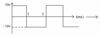
For an integrator circuit the output voltage is given by
vo = - I
I
vin = 10 v 0<t <1 ms (1)
vin = - 10v 1ms< t < 2 ms (2)
The required output is
Substituting equation (1) & (2) in (I) and calculating R1C1,
we get R1C1 =time constant = 0.5 s.
Q.2 Write the squared magnitude
Butterworth response and the second order normalised Butterworth polynomial.
Design a fourth order Butterworth LPF by cascading two second order
prototypes. Take the cut-off frequency as one kilohertz. (7)
Ans:
Squared magnitude response of a butterworth 2nd order
filter:

Second order normalized Butterworth polynomial:

Design of a fourth order Butterworth LPF
Fc = 1KHz
(a)Design of 2nd order LPF using sallen Key Topology:
Circuit:-

=
Cascading of 2 such stages to get a 4th order filter:-
Q.3 Find the
order of a Chebyshev filter with equiripple passband and following
specifications:
Passband ripple  2 dB;
2 dB;
Passband edge = 1 rad/sec;
Stopband attenuation  20 dB;
Stopband edge = 1.3 rad/sec. (6)
Ans:
Given :
min = 20 dB
max = 2dB
ws = 1.3 rad/s
wp = 1 rad/s
Order of given chebyshev filter can be found as

Q.4 Draw a neat sketch of a 3-bit
parallel comparator ADC. What are the reference levels set up for the
comparator by the reference voltage divider? Which are the components that
limit the conversion time? What type of ICs are recommended for flash
converters of 6-bits and UP? (10)
Ans:

Suppose the max analog input that can be measured be V volts
Then

Q.5 A third order
low pass filter has two transmission zeros at  and at infinity. Its natural modes are
at
and at infinity. Its natural modes are
at  and
and  . Find the value of
the transfer function if the d.c. gain is 5. (6)
. Find the value of
the transfer function if the d.c. gain is 5. (6)
Ans:
Zeroes
W = 2 rad/s
W= ¥
Poles (Natural modes)
S = - 0.5 + j0.8
S = - 0.5 –
j0.8
S = -1
Characteristic
equation is given by:-
Characteristic
Polynomial D(S) = (S+1) (S+0.5-j0.8) (S+0.5+j0.8 )=0
D(S)
=(S+1) (S2+1.2S+1)
= S3+2.2
S2+2.2 S+1
Now;
There
is a zero at W=2 or s= ±2j ( of conjugate symmetry)
=
N(S) = S2+2
Thus
T
(s) =  {
K corresponds to DC gain }
{
K corresponds to DC gain }
Putting
S=0 , we have T (S)= 5 (DC gain)
2K = 5
K = 

Q.6 The IC 741
OPAMP has a slew rate of 0.5V per microsecond. If this is to be used at a
frequency of 5.31 KHz, find the maximum undistortion sine wave amplitude.
(2)
Ans:
Slew rate 0.5 V/μs
Frequency 5.31 KHz
Slew Rate = 
Taking v= a coswt (a= amplitude, w= frequency)
We have slew rate =  =aw
=aw
a = 
= 
 V
V
Q.7 Design
a unity gain Low-pass active filter to meet the following specifications:
Roll off rate = - 40
dB/decade
Passband as flat as
possible
Cut off frequency = 2
KHz,
dc gain = 5. (5)
Ans:
Unity Gain LPF (Butterworth Response – Second order)
{ Roll-off rate = - 40 dB/decade}
Low pass prototype of 2nd order with
normalized frequency:-

Now,
De Normalizing to frequency wn (=3dB frequency) we have

We
require the gain to be unity at w= 2KHz
=


Design: Using sallen- key Topology we have the following circuit.

The flattest
passband comes from a Butterworth type filter, hence 
To obtain a DC gain of 5, we must add an amplifier with a gain of 5.
Q.8 The
parameters of a counter type ADC are given below:
Clock frequency = 1 MHz,
Comparator
threshold = 0.1 mV,
Full scale output
of DAC used = 10.23,
DAC input =
10-bits,
Find the following:
(i)
The digital equivalent obtained for an analog
input of 3.728 V.
(ii)
The conversion time.
(iii)
The resolution of the converter. (6)
Ans:
(i) 10.23 V = 210

Q.9 Design a second order
high-pass Butterworth active filter for a lower cut-ff frequency of 2.5
kilohertz. (7)
Ans:
Given cut off frequency of 2.5 KHz(HPF)
fL = 2.5 KHz
The voltage gain magnitude equation of the second order HPF is as
follows

Where Af = 1.586 pass band gain and f = frequency of the
input signal.

Let R2 = R3 = R and C2 = C3
= C = 0.01µf
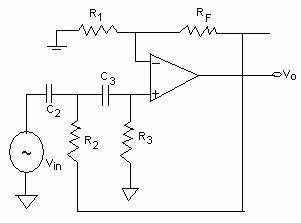

Let C = 0.01µf and the value of R will be

For RF and R1, Gain=1.586
 or
or 
Let R1=10K so RF=10K*0.586=5.86 K
Q.10 Determine the
cutoff frequency of an OPAMP, whose dc gain is 200 V/mV and unity gain
bandwidth is one megahertz. (3)
Ans:
We know for an OPAMP, gain bandwidth product is constant.
Also,
unity gain bandwidth = 1MHz
Hence,
Gain-Bandwidth product = 1MHz = 1 *106 Hz
Thus,
For
a gain of 200V/mV = 2 *105,
The
cut off frequency = Hz=5
Hz
Hz=5
Hz
Hence,
the cut off frequency for gain of 200 V/mV is 5 Hz.
Q.11 Design
a first order low-pass active filter to have a cut-off frequency of 15.9 kHz
and to provide a pass-band gain of 1.5. Write the designed filter circuit and
the expression for its transfer function (magnitude form). What is the
magnitude of the transfer function for the following input frequencies?
(i) 5 Hz (ii) 10 Hz
(iii) 100 Hz (iv)
1000 Hz (10)
Ans:
Pass-band gain=1.5, fH=15.9 KHz
Let C=0.01 μF then

=1 KΩ
Since the passband gain is 1.5

Let RF=10 KΩ and R1=20 KΩ

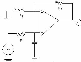
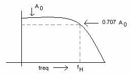

Putting the values for different frequencies, the transfer function
can be calculated.
Q.12 Design
a first order high-pass active filter for a cut-off frequency of 10 KHz
providing a pass-band gain of 1.5. Illustrate the circuit of the filter
designed and find the magnitude of the response for the following frequencies:
(i) 10 Hz (ii) 100 Hz
(iii) 500 Hz (iv)
1000 Hz (9)
Ans:
Transfer function for a first order high pass filter is 
Let a1=1

w0 is cut off frequency and is given by 1/CR w0
= 1/CR1 ----------------(2)
Given that fo = 10 KHz
wo = 2*3.14 fo = 2 × 3.14 ×10 × 103
= 62.8×10³ r/s.
High frequency gain = -R2/R1
Gain in the pass band is given as 1.5

Let C = 0.1 μF
Then from w0 = 
R1 =1.6 × 102 = 160 
From (3) R2 =160 × 1.58 = 240
Magnitude of the response for following frequencies:
i)
10 Hz
20
log  - 20
log
- 20
log 
=
20 log 


ii) 100 Hz = 20 log  -
-
iii) 500 Hz = 20 log  -20 log
iv) 1000 Hz = 20 log  - 20 log
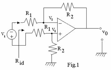
 where ii is the current drawn
from the source. Since the two input terminals of OPAMP track each other in
potential therefore writing loop equation-
where ii is the current drawn
from the source. Since the two input terminals of OPAMP track each other in
potential therefore writing loop equation-  . (B)
. (B)  .
. . (D)
. (D)  .
.

 . It represents a _________filter.
 the poles and zeros of this filter are
at
the poles and zeros of this filter are
at