Code: A-09/C-03/T-03 Subject: ANALOG & DIGITAL ELECTRONICS
Time: 3 Hours Max. Marks: 100
NOTE: There are 11 Questions in all.
· Question 1 is compulsory and carries 16 marks. Answer to Q. 1. must be written in the space provided for it in the answer book supplied and nowhere else.
· Answer any THREE Questions each from Part I and Part II. Each of these questions carries 14 marks.
· Any required data not explicitly given, may be suitably assumed and stated.
Q.1 Choose the correct or best alternative in the following: (2x8)
a.
Output voltage  of the circuit shown below is approximately
(A)  .
.
(B)  .
.
(C)  .
.
(D)  .
.
b. In switching capacitor circuit, the value of resistor corresponding to switched capacitor of value  and switching frequency 10 KHz is
(A)  . (B)
. (B)  .
.
(C)  . (D)
. (D)  .
.
c. A 7-M-byte memory chip has the capacity of
(A)  . (B)
. (B)  .
.
(C)  . (D)
. (D)  .
.
d. A successive approximation ADC has a resolution of 20 mV. The digital output for an analog input of 2.17 V is
(A) 01101101. (B) 01101011.
(C) 01110111. (D) 01101100.
e. A square wave with a period of 10  drives a T-flip-flop. The period of the output signal will be
(A)  . (B)
. (B)  .
.
(C)  . (D)
. (D)  .
.
f. In comparison to Bipolar op-amps, the MOS op-amps are
(A) superior in quality. (B) inferior in quality.
(C) quality is almost same. (D) much much superior in quality.
g. A high pass RC filter acts as a pure differentiator when
(A)  . (B)
. (B)  .
.
(C)  . (D)
. (D)  .
.
h. Boolean expression  is equal to
(A)  . (B)
. (B)  .
.
(C)  . (D)
. (D)  .
.
PART I
Answer any THREE Questions. Each question carries 14 marks.
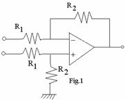
Q.2 a. Write biquadratic transfer function for lowpass, highpass, bandbass and band reject filters. (6)
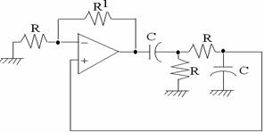
b. Using  verify that the circuit given in Fig.1 below is a band pass filter. (8)
Q.3 a. Derive the input impedance of a close loop non-inverting op-Amp. amplifier and show that it is greater than the open loop input impedance. (8)
b. What is an analog multiplier? Compare in brief, the performances of 1-quadrant, 2-quadrant and 4-quadrant multipliers. (6)
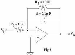
Q.4 a. Under what condition the circuit of Fig.2 can function as a log-amplifier? Use ideal op-amps. (8)
b. Draw an op-amp based sample and hold circuit and explain the operation. (6)
Q.5 a. Discuss the switching time of a transistor with the help of a pulse waveform at the input of a transistor. (4)
b. Draw the circuit of a 4-quadrant Gilbert multiplier and derive its output. State the approximation made, if any. (10)
Q.6 Write short notes on any TWO of the following :
(i) Slew rate of op-amp.
(ii) Dual slope type of ADC.
(iii) Instrumentation Amplifier.
(iv) Multiple op-amps Biquad filter. (7 x 2 = 14)
PART II
Answer any THREE Questions. Each question carries 14 marks.
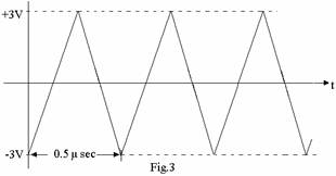
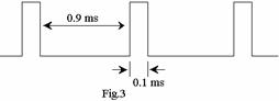
Q.7 a. Derive the necessary parameters to sketch and explain the transfer characteristic of the TTL circuit of Fig.3 below: - (8)
b. What are the problems associated with the interfacing of TTL with CMOS and Vice Versa? How can these problems be removed? (6)
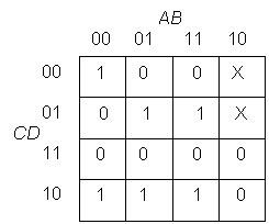
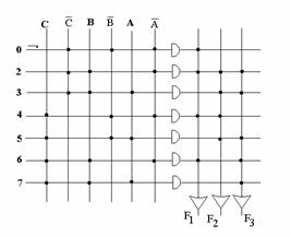
Q.8 a. Implement a simplest PLA circuit for the Boolean function given below. (8)

b. Compare PROM, PAL and PLA with an example for each. (6)
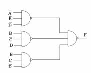
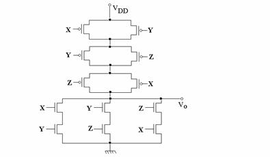
Q.9 a. Discuss the rule of formation of CMOS network for arbitrary combinational function. Using this rule form the CMOS network for the function f.  (8)
(8)
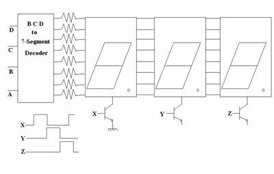
b. Design and explain a basic circuit to display a 3-digit number using only one 7-segment decoder. (6)
Q.10 a. Design a digital circuit to compare two numbers A and B having 2-bit each for three outputs A > B, A = B and A < B. Use only AND, OR NOT and NOR gates. (8)
b. Implement a full adder circuit with MUX modules. (6)
Q.11 Write short notes on any TWO of the following :
(i) Compare between TTL and ECL family.
(ii) Shift Registers.
(iii) Memory organization.
(iv) Synchronous vs Asynchronous counters. (7 x 2 = 14)
DETAILED SOLUTIONS A-09 DEC2003
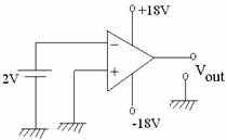
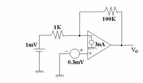
Q1.a. D The OpAmp is working as a comparator and its negative terminal
is at a higher potential than the positive terminal. Therefore, the
output will saturates to –18 volts, approximately.
b. B The equivalent resistance is equal to  where f = 10KHz and
 .
.
c. B 7x106 bytes = 7x8x106 bits.
d. D The binary number 01101100 = 108 (decimal) corresponds to input
voltage of 2.16 volts. It is the highest level smaller than 2.17 volts.
e. A If T-input is at logic 1, the output waveform has a period twice as
that of the input waveform.
f. A MOS Opamps have better linearity and better noise performance.
g. A The transfer function H(s) of an RC highpass filter is
 , which is proportional to s if
  .
.
h. D Apply Demorgan’s theorem once to write the give expression as
 . Apply Demorgan’s theorem once more to get the result.
PART I
Q2. a. For biquadratic transfer functions, refer to Table 12.16 [1]
b. With finite gain A, the negative input terminal of the Opamp will be at  .
.
KCL at this terminal can be written as
 , or
, or 
Substituting for  and simplifying gives the bandpass transfer
function as
 .
.
Q3.a. The figure below shows the circuit of noninverting amplifier. The Opamp has an
input impedance of Rin and the current flowing through it develops a small
voltage V with the polarity shown in the figure. The KCL equation at negative
terminal of Opamp can be written as

This can be simplified to

In a noninverting amplifier Vo is positive if Vs is positive. Thus, the input
impedance as seen by the positive terminal of Opamp is greater than Rin ,
the impedance of the open loop amplifier.
b. For analog multipliers, refer to Sections 16.13, 16.14 [2].
Q4.a. For details of the given logarithmic amplifier, refer to Section 16.13 [2].
The conditions are required for the circuit to be a logarithmic amplifier are:
(i) Q1 and Q2 should be matched transistors.
(ii) The transistors should be biased such that  and
and  .
.
(iii) The base voltage of Q2 be very small compared to VREF.
b. For Sample and Hold circuits, refer to Section 16.2 [2].
Q5.a. For transistor Switching times, refer to Section 3.8 [2].
b. For Gilbert multiplier, refer to Section 16.14 [2].
Q6. (i) For Slew rate of Opamps, refer to Section 2.6 [1].
(ii) For Dual Slope ADC, refer to Section 16.5 [2].
(iii) For Instrumentation Amplifier, refer to Section 2.4 [1].
(iv) For Multiple Opamp Biquad, refer to Section 12.7 [1].
PART II
Q7.a. For Transfer Characteristics of TTL, refer to Sections 6.5, 6.6, 6.7 [3].
b. For TTL-CMOS interfacing, refer to Section 8.12 [3].
Q8.a. A simple PLA implementation of the given functions is shown in figure below.
b. For PROM, refer to Section 11.6 [1]. For PAL and PLA, refer to Sections 7.14 and 7.15 [2].
Q9.a. For rule of CMOS gate formation, refer to Section 10.3 [1]. Using this rule, the following circuit for the given function results.
b. A circuit for a 3-digit display using using only one decoder is shown below. The
data to be displayed by the three displays comes in to the display decoder serially.
The displays are also turned ON serially (one at a time) by mutually exclusive
waveforms applied to the displays as shown in the figure. Thus, a single BCD to
7-segment decoder can be multiplexed to turn ON the three displays.
Q10.a. For description of a comparator circuit, refer to Section 7.4 [2].
b. The Boolean functions describing a full adder having A, B and C as inputs, are given as


The implementation using two 4:1 multiplexers is shown in the figure.

Q11. (i) For comparison between TTL and ECL, refer to Section 7.1 [3].
(ii) For Shift Registers, refer to Section 8.5 [2].
(iii) For Memory Organization, refer to Sections 12.16,12.17 [3].
(iv) For Synchronous and Asynchronous counters, refer to Sections 8.6,8.7 [2].
References
1. S.Sedra and K.C.Smith, “Microelectronic Circuits”, Saunders College Publishing, Fifth Edition, 2004.
2. J.Millman and A.Grabel, “Microelectronics”, McGraw-Hill International Edition, Second Edition, 1999.
3. H.Taub and D.Schilling,”Digital Integrated Electronics”, McGraw-Hill, 1977.
Code: A-09/C-03/T-03 Subject: ANALOG & DIGITAL ELECTRONICS
Time: 3 Hours Max. Marks: 100
NOTE: There are 11 Questions in all.
· Question 1 is compulsory and carries 16 marks. Answer to Q. 1. must be written in the space provided for it in the answer book supplied and nowhere else.
· Answer any THREE Questions each from Part I and Part II. Each of these questions carries 14 marks.
· Any required data not explicitly given, may be suitably assumed and stated.
Q.1 Choose the correct or best alternative in the following: (2x8)
a.
The circuit shown in the Fig.1 represents
(A) LPF.
(B) HPF.
(C) BPF.
(D) BSF.
b.
The frequency limit for the circuit shown in Fig.2 to operate as an integrator will be
(A) 1.6 Hz.
(B) 16 Hz.
(C) 160 Hz.
(D) 1.6 KHz.
c. The three basic second order filtering functions LP, BP and HP are performed simultaneously by a universal active filter that can be implemented using
(A) two integrator loop Biquad. (B) Second order LCR resonator.
(C) single amplifier Biquad. (D) both by (A) and (C).
d. The output of an op-amp voltage follower is a triangular wave shown in Fig.3 below, for a square wave input of frequency 2 MHz and 10 V peak to peak. The slew rate of the op-amp is
(A) 14  .
.
(B) 28 .
(C) 12 .
(D) 24 .
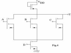
e. The circuit at Fig.4 gives an output Y given by
(A)  .
.
(B)  .
.
(C)  .
.
(D)  .
.
f. A 4 bit ripple counter has a count of 1001 at some instant. The count after 23 pulses will be
(A) 1001. (B) 0000.
(C) 1110. (D) 0110.
g. The problem of current hogging is associated with
(A) DTL. (B) ECL.
(C) TTL. (D) DCTL.
h. A ripple counter uses flip flops having tpd = 12 nsec. The largest mod counter that can be constructed from flip flops operated at 10 MHz is
(A) 128. (B) 256.
(C) 64. (D) 16.
PART I
Answer any THREE Questions. Each question carries 14 marks.
Q.2 a. What is the difference between open loop and closed loop gain of an Op-Amp? The dc open loop gain of an op-amp is  . What will be the open loop gain at its break frequency? (4)
b. Does increasing the compensating capacitor increase or decrease the unity factor bandwidth? How fast can the output of an op-amp change by 10 V, if its slew rate is 1 V/ . Also find the maximum frequency for a sine-wave output voltage of 10 V peak with an op-amp whose slew rate is 1 V/. (5)
c. For a non-inverting amplifier R =  ,
,  . The op-amp has the following specifications.

Assume that the amplifier is nulled at  . Calculate the value of the error voltage and the output voltage
  at
at  if
if  . (5)
. (5)
Q.3 a. Explain with a circuit diagram, a two - stage CMOS op-amp configuration. What is systematic offset? How can it be minimized? (7)
b. For an instrumentation amplifier, show that the output voltage is given by 
Where the symbols have usual significance. (7)
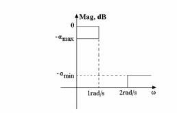
Q.4 Determine the ripple factor and order N of the network function that uses Chebyshev approximation to satisfy the following requirements

Compare the value of N with Butterworth approximation for same specifications. Derive the necessary expressions. (14)
Q.5 a. What is a flash converter? Explain. Consider the design of a 4 bit flash ADC. How many comparators are required? For an input signal in the range of 0 to +10V, what are the reference voltages needed? Show how they can be generated using a 10V reference and several 1 KW resistors. If a comparison is possible in 50 nsec and the associated logic requires 35 nsec, what is the maximum possible conversion rate? Indicate the digital code you expect at the output of the comparators and at the output of the logic for an input of
(i) 0V (ii) + 5 .1 V and (iii) +10 V. (10)
b. Write a note on IC power amplifiers. (4)
Q.6 With reference to any logic family, explain the following :
(i) Transfer characteristics.
(ii) Sourcing and sinking current.
(iii) DC Noise Margin and AC Noise Margin..
(iv) Totem pole TTL and Tristate TTL.
(v) Speed power product. (14)
PART II
Answer any THREE Questions. Each question carries 14 marks.
Q.7 a. Design a BCD to excess-3 code converter using a diode ROM circuit. (6)
b. Design a combinational circuit that converts a 4 bit reflected code number to a 4 bit binary number. Implement the circuit with exclusive OR gates. (8)
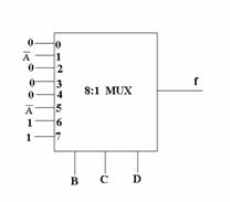
Q.8 a. Signals A, B, C, D and  are available. Using only one 8 : 1 MUX and no other gates, implement the function,
 (7)
(7)
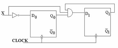
b. A clocked sequential circuit has 3 states A, B, C and input X. As long as X = 0, the circuit alternates between states A and B. If X becomes 1 (either in state A or B), circuit goes to state C and remains in state C as long as X = 1. The circuit goes to state A if X becomes 0 again and then repeats the behaviour. Assume state assignments as A = 00, B = 01 and C = 10.
(i) Draw the state diagram.
(ii) Prepare the state table.
(iii) Draw the circuit using D flip flops. (7)
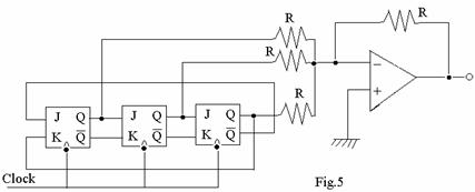
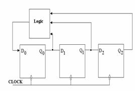
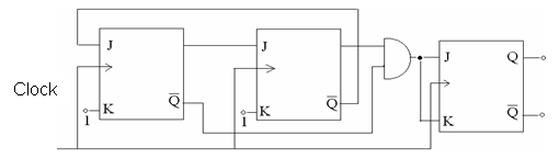
Q.9 a. For the circuit shown in Fig.5 below, sketch  against time. Assume that all flip flops are reset to zero before the clock is applied. (8)
b. (i) How many flip flops are required to build a binary counter circuit to count from 0 to 1023?
(ii) What is the frequency of the output of last flip flop for an input clock frequency of 5 MHz?
(iii) What is the counter’s MOD number?
(iv) If the counter is initially at zero, what will it hold after 2060 pulses?
(v) Does the maximum frequency of a counter depend on the modulus for
· Synchronous counter?
· Ripple counter?
Explain. (6)
Q.10 a. What is the difference between a 2D organised memory and  organisation? Illustrate the memory organisation for a 16 word, 1 bit / word memory. (7)
b. Explain the difference between PLD, PAL and PLA. (3)
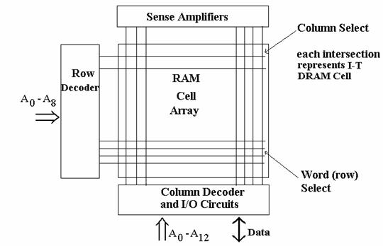
c. Illustrate with a block diagram,  DRAM organisation using 8192 column 512 row cell array. (4)
Q.11 Write explanatory notes on any TWO :
(i) Sequence Generators.
(ii) Single Amplifier Biquad.
(iii) Analog Multipliers.
(iv) Switched capacitor filters. (7 x 2 = 14)
Detailed Solution A-09 June 2004
|
|
Q1.a. D The output Vo is equal to V+ (the voltage at the positive terminal of
the OpAmp) for both  (both capacitors are open circuit) and
 (both capacitors are short circuit). This is not possible for
LPF or HPF or BPF .
b. C The transfer function of the integrator is  . Its Bode
plot has a corner frequency at 100 rad/s or 16 Hz. Thus limiting
frequency should be ten times 16 Hz = 160 Hz.
c. A Refer to Section 12.7 [1]
d. D From the figure, slew rate = .
.
e. B Transistor D is in series with parallel combination of transistors
A, B and C. Thus, the result.
f. B After 16 pulses the counter will come back to the state it started
with (1001). Another 7 pulses will take it to 0000.
g. D Refer to Section 4.3 [3].
h. B The time taken for the input pulse to ripple through all the N flip-
flops will be 12N nsec. Thus, the maximum speed of operation of
the counter is 1/(12x10-9N).

or N=8. Therefore modulo count is 2N=256.
PART I
Q2. a. Refer to Sections 2.1, 2.2 [1].
Gain at corner frequency is equal to Open loop gain (in dB) – 3dB. If the open
loop gain is 105, then gain at corner frequency = 20log10105 – 3 = 97 dB.
b. Compensating capacitor avoids oscillations in an amplifier by reducing its gain at a frequency at which the phase shift is 1800. Such compensating capacitor introduces an additional pole at a frequency much lower than the frequencies of the natural poles of the amplifier. As such, the gain of the amplifier drops to unity at a smaller frequency.
If the slew rate is  , the smallest duration in which the output can change by 10V is
  .
.
Maximum frequency of sine wave =
c. For 10 degree change in temperature, the offset voltage will be while the
offset current will be 3nA. Thus, the Op-Amp inverter with input voltage, offset
voltage and offset current is as shown in the figure below. The output voltage is
obtained by writing KCL at the inverting terminal as
 .
.
Thus,  and the error = 29.4mV.
Q3.a. For two-stage CMOS Op-Amp, refer to Section 9.1 [1].
b. For instrumentation amplifier, refer to Example 2.4 [1].
Q4. For details on Butterworth and Chebyshev filters, refer to Section12.3 [1].
With reference to the figure shown, the ripple factor  can be evaluated from
 .
.
Thus,  . The order NCH of the Chebyshev filter can be obtained from the following equation, with
  , as
, as

The order must be an integer. Thus NCH = 4. Similarly, the order NBW of the Butterworth filter having same specifications can be obtained from the following equation as
 ,
,
or NBW = 6, which is 2 higher than the order used for Chebyshev filter.
Q5.a. The flash analog to digital converter is the fastest conversion method. A 4-bit
flash converter uses 24-1=15 comparators. The analog input Va is applied to the
positive terminal of each comparator. The negative terminal of the comparators
is supplied with equally spaced reference voltages obtained from a potential
divider network consisting of 24=16 1K resistances as shown in the figure below.
This arrangement sorts the analog input in a range between two adjacent reference
voltages. The outputs of the comparators are fed to a priority encoder to obtain the binary output. The required fifteen reference voltages are  .
.
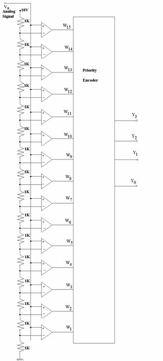
Inputs |
Outputs |
W15 |
W14 |
W13 |
W12 |
W11 |
W10 |
W9 |
W8 |
W7 |
W6 |
W5 |
W4 |
W3 |
W2 |
W1 |
Y3 |
Y2 |
Y1 |
Y0 |
0 |
0 |
0 |
0 |
0 |
0 |
0 |
0 |
0 |
0 |
0 |
0 |
0 |
0 |
0 |
0 |
0 |
0 |
0 |
0 |
0 |
0 |
0 |
0 |
0 |
0 |
0 |
0 |
0 |
0 |
0 |
0 |
0 |
1 |
0 |
0 |
0 |
1 |
0 |
0 |
0 |
0 |
0 |
0 |
0 |
0 |
0 |
0 |
0 |
0 |
0 |
1 |
1 |
0 |
0 |
1 |
0 |
0 |
0 |
0 |
0 |
0 |
0 |
0 |
0 |
0 |
0 |
0 |
0 |
1 |
1 |
1 |
0 |
0 |
1 |
1 |
0 |
0 |
0 |
0 |
0 |
0 |
0 |
0 |
0 |
0 |
0 |
1 |
1 |
1 |
1 |
0 |
1 |
0 |
0 |
0 |
0 |
0 |
0 |
0 |
0 |
0 |
0 |
0 |
0 |
1 |
1 |
1 |
1 |
1 |
0 |
1 |
0 |
1 |
0 |
0 |
0 |
0 |
0 |
0 |
0 |
0 |
0 |
1 |
1 |
1 |
1 |
1 |
1 |
0 |
1 |
1 |
0 |
0 |
0 |
0 |
0 |
0 |
0 |
0 |
0 |
1 |
1 |
1 |
1 |
1 |
1 |
1 |
0 |
1 |
1 |
1 |
0 |
0 |
0 |
0 |
0 |
0 |
0 |
1 |
1 |
1 |
1 |
1 |
1 |
1 |
1 |
1 |
0 |
0 |
0 |
0 |
0 |
0 |
0 |
0 |
0 |
1 |
1 |
1 |
1 |
1 |
1 |
1 |
1 |
1 |
1 |
0 |
0 |
1 |
0 |
0 |
0 |
0 |
0 |
1 |
1 |
1 |
1 |
1 |
1 |
1 |
1 |
1 |
1 |
1 |
0 |
1 |
0 |
0 |
0 |
0 |
0 |
1 |
1 |
1 |
1 |
1 |
1 |
1 |
1 |
1 |
1 |
1 |
1 |
1 |
1 |
1 |
0 |
0 |
0 |
1 |
1 |
1 |
1 |
1 |
1 |
1 |
1 |
1 |
1 |
1 |
1 |
1 |
1 |
0 |
0 |
0 |
0 |
1 |
1 |
1 |
1 |
1 |
1 |
1 |
1 |
1 |
1 |
1 |
1 |
1 |
1 |
1 |
0 |
1 |
0 |
1 |
1 |
1 |
1 |
1 |
1 |
1 |
1 |
1 |
1 |
1 |
1 |
1 |
1 |
1 |
1 |
1 |
0 |
1 |
1 |
1 |
1 |
1 |
1 |
1 |
1 |
1 |
1 |
1 |
1 |
1 |
1 |
1 |
1 |
1 |
1 |
1 |
The logic for the priority encoder can be obtained as per the following truth table.
If time taken for comparison is 50ns and that for priority encoder is 35ns, then total time for conversion is 85ns. Thus, the maximum possible conversion rate is  .
.
The output Y3Y2Y1Y0 for inputs 0V, 5.1V and 10V will be, respectively, 0000, 1010 and 1111.
b. For IC power amplifiers, refer to Section 14.8 [1]
Q6. For TTL, refer to Sections 6.5, 6.6, 6.7, 6.10 [3].
Q7.a. The truth table for BCD to Excess-3 code is shown in the truth table given below.
ROM Address |
ROM Outputs |
W4 |
W3 |
W2 |
W1 |
Y3 |
Y2 |
Y1 |
Y0 |
0 |
0 |
0 |
0 |
0 |
0 |
0 |
0 |
0 |
0 |
0 |
1 |
0 |
0 |
0 |
1 |
0 |
0 |
1 |
0 |
0 |
0 |
1 |
0 |
0 |
0 |
1 |
1 |
0 |
0 |
1 |
1 |
0 |
1 |
0 |
0 |
0 |
1 |
0 |
0 |
0 |
1 |
0 |
1 |
0 |
1 |
0 |
1 |
0 |
1 |
1 |
0 |
0 |
1 |
1 |
0 |
0 |
1 |
1 |
1 |
0 |
1 |
1 |
1 |
1 |
0 |
0 |
0 |
1 |
0 |
0 |
0 |
1 |
0 |
0 |
1 |
1 |
0 |
0 |
1 |
The table also shows the excess-3 outputs of the ROM for different BCD inputs
given as ROM address. The data stored in the ROM for remaining inputs is don’t
care.
b. For truth table of Gray to binary converter, refer to Section 7.9 [2]. The corresponding Boolean functions can be obtained from this table as

which can be easily implemented using Ex-OR gates.
Q8a.The residues of the given Boolean function for various combinations of B, C and D are shown in the following truth table, which can be implemented by an 8:1 MUX as shown in the figure
B |
C |
D |
f |
0 |
0 |
0 |
0 |
0 |
0 |
1 |

|
0 |
1 |
0 |
0 |
0 |
1 |
1 |
0 |
1 |
0 |
0 |
0 |
1 |
0 |
1 |
|
1 |
1 |
0 |
1 |
1 |
1 |
1 |
1 |
b. The state diagram for the problem and the state table along with D inputs of the two flipflops are as shown below.
PS |
NS |
D1 |
D0 |
Q1Q0 |
X=0 |
X=1 |
0 1 |
0 1 |
0 0 |
0 1 |
1 0 |
0 1 |
1 0 |
0 1 |
0 0 |
1 0 |
0 0 |
1 0 |
1 0 |
0 0 |
1 0 |
0 0 |
1 0 |
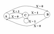
From the table,  and
and  . The circuit is as given below.
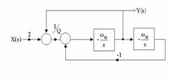
Q9.a. The given circuit is a modulo-6 twisted ring (Johnson) counter, whose outputs Q0, Q1, Q2 are fed to an inverting summer amplifier. Count sequence of the counter is 000,100,110,111,011,001. Therefore, the output of the Opamp will be a repeating sequence 0V, -1V, -2V, -3V, -2V, -1V changing at every falling edge of the clock. as shown in the figure.

b. (i) 10
(ii) (5/1024) MHz, assuming a ripple counter.
(iii) 1024
(iv) 2060=1024+1024+12. Hence, counter will hold 12.
(v) Yes, in case of a ripple counter. In a synchronous counter, the clock is applied simultaneously to all flipflops and thus, the maximum frequency of operation does not depend on the modulus of the counter.
Q10.a. A 2½ D organized 16X1 memory is using two 2-4 decoders is shown in the figure below.
b. For programmable arrays, refer to Sections 7.14, 7.15 [2].
c.
Q11. (i) For sequence generators, refer to Section 10.17 [3].
(ii) For Single Amplifier Biquad , refer to Section 16.10[2].
(iii) For analog multipliers, refer to Sections 16.13, 16.14 [2]
(iv) For Switched Capacitor Filters, refer to Section 16.12 [2].
References
1. S.Sedra and K.C.Smith, “Microelectronic Circuits”, Saunders College Publishing, Fifth Edition, 2004.
2. J.Millman and A.Grabel, “Microelectronics”, McGraw-Hill International Edition, Second Edition, 1999.
3. H.Taub and D.Schilling,”Digital Integrated Electronics”, McGraw-Hill, 1977.
Code: A-09/C-03/T-03 Subject: ANALOG & DIGITAL ELECTRONICS
Time: 3 Hours Max. Marks: 100
NOTE: There are 11 Questions in all.
· Question 1 is compulsory and carries 16 marks. Answer to Q. 1. must be written in the space provided for it in the answer book supplied and nowhere else.
· Answer any THREE Questions each from Part I and Part II. Each of these questions carries 14 marks.
· Any required data not explicitly given, may be suitably assumed and stated.
Q.1 Choose the correct or best alternative in the following: (2x8)
a. The magnitude response  of a Butterworth filter of order N has maximally flat characteristics because
(A) first N derivatives of are equal to 0 at  .
.
(B) first N-1derivatives of are equal to 0 at .
(C) first N-1 derivatives of are equal to 0 at  .
.
(D) first N derivatives of are equal to 0 at .
b.
Input impedance of the OpAmp circuit shown in the fig.1 is
(A) 
(B)  .
.
(C)  .
.
(D)  .
.
c. Output  for
for  dc for the circuit
shown in the fig.2 will be
(A) 1.0 V.
(B) -0.5 V.
(C) 0.5 V.
(D) 0.0 V.
d. The Boolean expression  can equivalently be written, in terms of its minterms, as
(A)  . (B)
. (B)  .
.
(C)  . (D)
. (D)  .
.
e. The T-input of a negative edge triggered has been tied to logic ‘1’. If its clock input is as shown in the fig.3, then ON and OFF time of its  out will be, respectively
(A) 0.2 ms and 1.8 ms.
(B) 1.8 ms and 0.2 ms.
(C) 0.5 ms and 0.5 ms.
(D) 1.0 ms and 1.0 ms.
f. Immediately after the inputs to a NAND RS flipflop are simultaneously switched from 00 to 11, the output Q of the flipflop will
(A) be equal to ‘0’. (B) be equal to ‘1’.
(C) race around. (D) be unpredictable.
g. The circuit shown in the fig.4 is a
(A) flipflop.
(B) sequential circuit.
(C) combinational circuit.
(D) parity checker.
h. A MOS differential amplifier has a large gain because
(A) the current through each driver transistor is a constant.
(B) sum of currents through both driver transistors is a constant.
(C) the load is a current source and offers a large resistance.
(D) there is a no feedback in the circuit.
PART I
Answer any THREE Questions. Each question carries 14 marks.
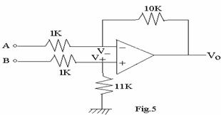
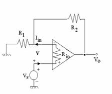
Q.2 The OpAmp shown in the circuit of fig.5 has an open loop gain of 10000, input impedance of 1MΩ and an output impedance of 1KΩ.
(i) Determine  if –2.1V is applied between terminals A and B. (5)
(ii) Find the gain  of this amplifier. (5)
(iii) Find the gain of the amplifier when the input has a source resistance of 1KΩ. (4)
Q.3 Consider the function  .
.
(i) Draw its pole-zero diagram. (2)
(ii) Sketch magnitude and phase responses of this function. (4)
(iii) For K=1, draw a passive circuit to realize H(s). (5)
(iv) Draw a block diagram circuit to realize this function using integrators, summers and multipliers. (3)
Q.4 Explain the working of a 12-bit dual-slope analog to digital converter using appropriate diagrams and derive the relevant expression for the digital output. If the input voltage is in range (0V, 10V) and the counter in the converter is given a clock of 1 MHz, determine
(i) the time taken for output of the integrator to reach its maximum value. (8)
(ii) conversion time for input voltage = 5V, assuming reference voltage of –10V. (6)
Q.5 a. Through proper sketches explain the electron density distribution in the base of a n-p-n Bipolar Junction Transistor when
(i) in Active region
(ii) in Saturation.
How will the explanation be different for a p-n-p transistor? (6)
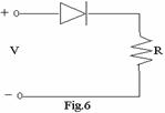
b. The input voltage V switches from +5V to –10V in diode circuit shown in the fig.6. Sketch the current through the diode and explain various regions of this waveform. (8)
Q.6 With short notes on any TWO of the following:
(i) DC level shifting in OpAmps.
(ii) Sample-and-Hold circuits and their applications.
(iii) Sensitivity of a single OpAmp Biquad.
(iv) MOS operational amplifiers. (14)
PART II
Answer any THREE Questions. Each question carries 14 marks.
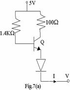
Q.7 a. A portion of TTL gate circuit is shown in the Fig.7(a), where the transistor Q has  Base-to-emitter voltage of the transistor is equal to 0.7V when it is in active region and 0.75V when Q is in saturation. Determine the output voltage V if the current I=2.5mA. (6)
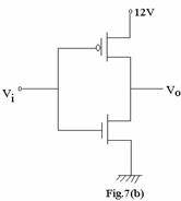
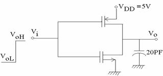
b. Both NMOS and PMOS transistors in the circuit of Fig.7(b) have a threshold voltage of 2V and equal characteristic constants. Determine the value of input voltage  and the range of output voltage for which both transistors will be in saturation. (8)
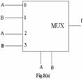
Q.8 a. Determine the Boolean function implemented by the multiplexer circuit shown in the fig.8 (a). (4)
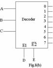
b. A 3-to-8 decoder has two enable inputs E1 and  as shown in fig.8 (b). Write a truth table showing the outputs
  in terms of inputs
  . (5)
. (5)
c. With the help of a diagram using Full-adders, explain the working of a 4-bit parallel addition/subtraction of 2’s complement numbers. (5)
Q.9 a. Explain the working of a positive-edge-triggered Master-Slave JK flipflop. What are its advantages over a normal JK flipflop? If all NAND gates used in the flipflop have a propagation delay of 5 ns, compute the delay of the Master-Slave. (6)
b. Design a circuit to generate the sequence 100010 using JK flipflops and logic gates as required. (8)
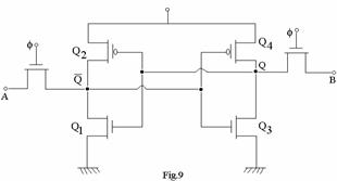
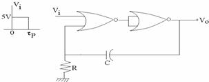
Q.10 a. What is the function of the circuit shown in the fig.9? Explain its working. (4)
b. Draw the circuit of a CMOS static RAM cell and explain its operation. (4)
c. Three negative edge triggered flipflops having inputs  ,
,  and
and  respectively, are connected to make a counter such that
Starting with  , what sequence(s) of states will the counter go through? (6)
Q.11 Write short notes on any THREE of the following:
(i) Emitter-Coupled OR gate.
(ii) CMOS logic gates.
(iii) BJT inverter.
(iv) Schottky diodes and its applications in digital circuits. (14)
DETAILED SOLUTIONS A-09 DEC 2004
Q1. a. B Refer to Section 16.9 [2]. The correct answer is B with 2N-1
instaed of N-1
b. C By virtual ground, the input terminals of the Opamp are at same
potential thus making resistances R1 in series.
c. C The capacitors are open circuit at dc and the voltage at the
inverting terminal of Opamp is the same as that at the noninverting
terminal (equal to 0.5V). Since no current flows feedback resistances, the output voltage is also equal to 0.5V.
d. A The function can be expanded as

e. D A T flipflop divides the frequency of the input clock by 2 and its
output is a square wave.
f. D When inputs are 00, both outputs are 1. Switching the input to 11
makes one of the outputs race to 0 .
g. B Because there is a feedback.
h. C The load in a MOS differential amplifier is very large, often a
current source.
PART I
Q2.a. With Opamp replaced by its equivalent circuit, the given amplifier can be drawn as shown in the figure where Vi = -2.1V. The node equations at negative and positive terminals of the Opamp may be respectively written as

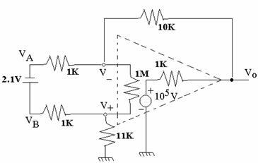
where V=V+-V- and A=105. Solving these equations with  gives V=0.231mV.
b. Same figure can be used to obtain the gain. Neglecting current through 1M input impedance of the Opamp, the node equations can be written as

Which give  . Further, the following equations may be written for currents through the three 1K resistances.

These two equations can be solved to get  . Substituting for AV gives
  . Thus, the gain is 10.5.
c. Same figure can be used to obtain the gain. Writing KVL for the loop containing the source, we get

where  is the source voltage and
  =1K is the source resistance. Using the result of Q2c gives
 .
.
Thus, the gain is 3.5.
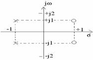
Q3. (i) The poles and zeros of H(s) are respectively given by
 and
and 
Thus, the poles are at mirror image locations of the zeros as shown in the
figure.
(ii) The magnitude of this allpass filter is K. For plots of magnitude and phase, refer to p.1105 [1].
(iii) For passive realization, refer to Section 12.5.7 [1].
(iv) With  , H(s) can be written as

Or, 
which can be realized as shown in the figure below.
Q4. For a description of Dual slope converter and derivation of expressions, refer to
Section 16.5 [2].
(i) Time required for the out put to reach its maximum value is same as the
time required by the counter to reach its maximum count of 212. For a clock of 1MHz, this is equal to  .
.
(ii) For a 5V input,  . Thus, conversion time is equal to t1+t2 = 6.144ms.
Q5.a. For electron density distribution and explanation, refer to Section 1.20 [3].
- For diode switching, refer to Section 1.18 [3]
Q6. (i) For DC level shifting, refer to Section 14.4 [2].
(ii) For Sample and Hold circuits, refer to Section 16.2 [2].
(iii) For Sensitivity of a Biquad, refer to Section 12.9 [1].
(iv) For MOS Opamps, refer to Section 14.13[2].
PART II
Q7.a. Assuming Q to be in active region, base current of Q = I/100 = 2.5x10⁻⁵A.
Thus,  V. It is easily seen that the collector
voltage is 5-ICRC=5-0.25=4.75V. and the base voltage is 3.25+0.7+0.7=4.65V.
Thus, VBC = -0.1V indicating that Q is indeed in active region.
- A trivial solution is when Vi < 2 volts and Vo = 12 volts.
Assume both transistors are in saturation. Then

Solving with kp=kn and VT = 2 volts, gives Vi = 6 volts.
PMOS will be in saturation if Vo - Vi < VT , or Vo < 8 volts. Also, NMOS will be in saturation if Vi - Vo < VT , or Vo > 4 volts. The range when both transistors are in saturation is 4< Vo <8.
Q8.a. It is easily seen that for AB equal to 00, 01, 10, 11, the output of multiplexer will
0, 1, 1, 1, respectively. Thus f = A+B.
- The required table is shown below
A B C D E |
O0 O1 O2 O3 O4 O5 O6 O7 |
x x x 0 x
x x x 0 x
0 0 0 0 1
0 0 1 0 1
0 1 0 0 1
0 1 1 0 1
1 0 0 0 1
1 0 1 0 1
1 1 0 0 1
1 1 1 0 1 |
0 0 0 0 0 0 0 0
0 0 0 0 0 0 0 0
1 0 0 0 0 0 0 0
0 1 0 0 0 0 0 0
0 0 1 0 0 0 0 0
0 0 0 1 0 0 0 0
0 0 0 0 1 0 0 0
0 0 0 0 0 1 0 0
0 0 0 0 0 0 1 0
0 0 0 0 0 0 0 1 |
Q9.a. For an explanation of Master-Slave JK flipflop and its advantages, refer to Section 8.4 [2]. A NAND flipflop will take 2 gate delays to stabilize the output after the inuts are applied. Thus, both Master and Slave sections of the flipflop require 3 gate delays. Add 1 gate delay for the gate used for complementing the clock. Thus the delay required after the positive edge of the clock is 4 gate delays or 20ns.
b. A sequence generator is a shift register whose first flipflop gets its D-input from the present state of the shift register through a combinational logic as shown in the figure below. The output of a flipflop in this circuit is a delayed version of its predecessor flipflop. This makes the truth table of the logic block as shown below. From the truth table the Boolean function for the sequence generator can be found to be  .
.
Q0 Q1 Q2 |
f |
0 0 0
0 0 1
0 1 0
0 1 1
1 0 0
1 0 1
1 1 0
1 1 1 |
0
0
0
0
0
0
0
0 |
Q10.a. For description of given circuit, refer to Section 11.4 [1].
b. For static RAM Cell, refer to Section 9.5 [2].
c. The following table derives the operational sequence of the counter, assuming K2 = 1 and J2 = Q0.
PS
Q0 Q1 Q2 |
J0 K0 J1 K1 J2 K2 |
NS
Q0 Q1 Q2 |
0 0 0
1 1 0
0 0 1
0 1 0
1 0 0
0 1 1 |
1 1 1 1 0 1
1 1 1 1 1 1
0 1 1 1 0 1
1 1 1 1 0 1
1 1 1 1 1 1
0 1 1 1 0 1 |
1 1 0
0 0 1
0 1 0
1 0 0
0 1 1
0 0 0 |
Thus, it is a mod-6 counter.
Q11. (i) For Emitter-coupled OR gate, refer to Section 7.2 [3].
(ii) For CMOS logic gates, refer to Section 10.3 [1].
(iii) For BJT inverter, refer to Section 6.10 [2].
(iv) For Schottky diode, refer to Section 1.19 [3]
References
1. S.Sedra and K.C.Smith, “Microelectronic Circuits”, Saunders College Publishing, Fifth Edition, 2004.
2. J.Millman and A.Grabel, “Microelectronics”, McGraw-Hill International Edition, Second Edition, 1999.
3. H.Taub and D.Schilling,”Digital Integrated Electronics”, McGraw-Hill, 1977.
 , or
, or 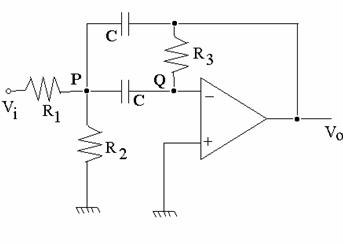

 .
.