Code: D-09 Subject: DIGITAL ELECTRONICS
Time: 3 Hours June 2006 Max. Marks: 100
NOTE: There are 9 Questions in all.
· Question 1 is compulsory and carries 20 marks. Answer to Q. 1. must be written in the space provided for it in the answer book supplied and nowhere else.
· Out of the remaining EIGHT Questions answer any FIVE Questions. Each question carries 16 marks.
· Any required data not explicitly given, may be suitably assumed and stated.
Q.1 Choose the correct or best alternative in the following: (2x10)
a. The hexadecimal number for ![]() is
is
(A)
![]() (B)
(B)
![]()
(C)
![]() (D)
(D)
![]()
b. The octal equivalent of ![]() is
is
(A)
![]() (B)
(B)
![]()
(C) ![]() (D)
(D)
![]()
c. The chief reason why digital computers use complemented subtraction is that it
(A) simplifies the circuitry.
(B) is a very simple process.
(C) can handle negative numbers easily.
(D) avoids direct subtraction.
d. In a positive logic system, logic state 1 corresponds to
(A) positive voltage (B) higher voltage level
(C) zero voltage level (D) lower voltage level
e. The commercially available 8-input multiplexer integrated circuit in the TTL family is
(A) 7495. (B) 74153.
(C) 74154. (D) 74151.
f. CMOS circuits are extensively used for ON-chip computers mainly because of their extremely
(A) low power dissipation. (B) high noise immunity.
(C) large packing density. (D) low cost.
g. The MSI chip 7474 is
(A) dual edge triggered JK flip-flop (TTL).
(B) dual edge triggered D flip-flop (CMOS).
(C) dual edge triggered D flip-flop (TTL).
(D) dual edge triggered JK flip-flop (CMOS).
h. Which of the following memories stores the most number of bits
(A)
a 5M![]() 8 memory. (B)
a 1M
8 memory. (B)
a 1M ![]() 16
memory.
16
memory.
(C) a ![]() memory. (D)
a
memory. (D)
a ![]() memory.
memory.
i. The process of entering data into a ROM is called
(A) burning in the ROM (B) programming the ROM
(C) changing the ROM (D) charging the ROM
j. When the set of input data to an even parity generator is 0111, the output will be
(A) 1 (B) 0
(C) Unpredictable (D) Depends on the previous input
Answer any FIVE Questions out of EIGHT Questions.
Each question carries 16 marks.
Q.2 a. Briefly explain the following:
(i) Binary number system.
(ii) Signed binary numbers. (7)
b. Perform the following operations using the 2’s complement method:
(i) 23 – 48 (ii) – 48 – 23 (4)
c. Write the schematic of a full subtractor in block diagram form. Explain how a full subtractor can be implemented using two half subtractors and OR gate. (5)
Q.3 a. Distinguish between combinational logic circuits and sequential logic circuits. How are the design requirements of combinational circuits specified? (7)
b. Prove the following Boolean identities using the laws of Boolean algebra:
(i) ![]()
(ii) ![]() (4)
(4)
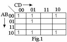
c. The Karnaugh map for a SOP function is given below in Fig.1. Determine the simplified SOP Boolean expression. (5)
Q.4 a. What are the characteristics of digital ICs used to compute their performance? Briefly describe the operation of DTL Nand gate (3-input gate) driving N similar stages. (11)
b. Explain the operation of a CMOS inverter. (5)
Q.5 a. What is a digital multiplexer? Illustrate its functional diagram. Write the scheme of a 4-input multiplexer using basic gates (AND/OR/NOT) and explain its operation. (8)
b. What is meant by a priority encoder? Name the 7400 series TTL chip which is a priority encoder. Write its truth table. Illustrate how it can be used as a decimal-to-BCD encoder. (8)
Q.6 a. What is a flip-flop? Write the truth table for a clocked J-K flip-flop that is triggered by the positive-going edge of the clock signal. Explain the operation of this flip-flop for the following conditions.
|
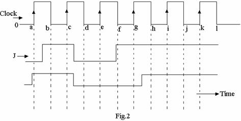
Initially all inputs are zero and assume the ‘Q’ output to be 1. (10)
b. What is chattering as applied to mechanical switches used in digital systems and why do they occur? What is its effect on the functioning of a sequential circuit? (6)
Q.7 a. How
is it possible to make a modulo ![]() counter using N-flipflops? Name the
two types of such counters and define each one of them. Illustrate the
counting sequence of a 3-bit binary counter and explain how this can be
realised using T-type flip-flops. (11)
counter using N-flipflops? Name the
two types of such counters and define each one of them. Illustrate the
counting sequence of a 3-bit binary counter and explain how this can be
realised using T-type flip-flops. (11)
b. A certain memory has a
capacity of 4K![]() 8
8
(i) How many data input and data output lines does it have?
(ii) How many address lines does it have?
(iii) What is its capacity in bytes? (5)
Q.8 a. In applications where the required memory capacity cannot be satisfied by a single available memory IC chip, what should the designer do to meet this requirement? (10)
b. A 5-bit DAC produces an output voltage of 0.2V for a digital input of 00001. Find the value of the output voltage for an input of 11111. What is the resolution of this DAC? Describe the staircase signal out of this DAC. (6)
Q.9 a. With a neat block schematic for illustration, explain the operation of a dual-slope ADC. (12)
b. An 8-bit successive approximation ADC has a resolution of 20mV. What will be its digital output for an analog input of 2.17V? If the clock frequency is 500KHz, what is the maximum conversion time of the converter? (4)