Code: D-08 Subject: ANALOG ELECTRONICS
Time: 3 Hours June 2006 Max. Marks: 100
NOTE: There are 9 Questions in all.
· Question 1 is compulsory and carries 20 marks. Answer to Q. 1. must be written in the space provided for it in the answer book supplied and nowhere else.
· Out of the remaining EIGHT Questions answer any FIVE Questions. Each question carries 16 marks.
· Any required data not explicitly given, may be suitably assumed and stated.
Q.1 Choose the correct or best alternative in the following: (2x10)
a. In a transistor amplifier with CB configuration.
(A) the current is high and voltage gain is low.
(B) both current and voltage gains are high.
(C) current gain is low and voltage gain is high
(D) both current and voltage gains are low.
b. If the CE h-parameters at low frequencies are known at a given
collector current, then the conductance ![]() in the hybrid-pi model can be
calculated using the equation
in the hybrid-pi model can be
calculated using the equation
(A)
![]() (B)
(B)
![]()
(C) ![]() (D)
(D)
![]()
c. The bias stability factor for a CE circuit is
(A)
1. (B)
![]() .
.
(C) ![]() . (D)
. (D)
![]() .
.
d. The maximum possible conversion efficiency in percent for a class-B power amplifier system is
(A)
![]() . (B)
. (B)
![]() .
.
(C) ![]() . (D)
. (D)
![]() .
.
e. Comparators are made using
(A) closed-loop operation.
(B) open-loop operation.
(C) any of the closed-loop or open-loop operations.
(D) none of the above.
f. The high-pass
second order filter is obtained from the low-pass second order prototype of
transfer function  where
where ![]() is the high-frequency 3-dB point, by
applying the transformation
is the high-frequency 3-dB point, by
applying the transformation
(A)

(B)

(C) 
(D) 
g. If a square wave is fed to a differentiating circuit, the output will be
(A) Sharp narrow pulses (B) Triangular wave
(C) Saw tooth wave (D) Sine wave
h. The best location for setting a Q-point on the dc load line of an FET amplifier is at
(A) saturation point. (B) cut-off point.
(C) mid point. (D) none of the above.
i. In a transistor
Colpitt’s oscillator, if ![]() ,
, ![]() and
and ![]() , the required gain for oscillations
will be
, the required gain for oscillations
will be
(A) 5. (B) 7.2.
(C) 13.7. (D) 10.
j. Stagger tuning in tuned amplifiers is achieved by using
(A) a double tuned circuit.
(B) tuned circuits which are tuned to the same frequency.
(C) tuned circuits which are tuned to slightly different frequencies.
(D) none of the above.
Answer any FIVE Questions out of EIGHT Questions.
Each question carries 16 marks.
Q.2 a. Which are the commonly used methods for biasing the transistors? (5)
b. A
transistor with ![]()
![]() ,
, ![]() and
and ![]() is used in a
biasing circuit as shown in Fig.1. It is desired to establish the quiescent
point at
is used in a
biasing circuit as shown in Fig.1. It is desired to establish the quiescent
point at ![]() and
stability factor
and
stability factor ![]() .
.
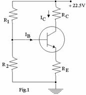
Find
the values of resistors ![]() . (11)
. (11)
Q.3 a. Draw the hybrid-pi model for transistor in CE configuration and briefly explain the components of the model. (8)
b. Draw the equivalent
circuit for frequency analysis of a CE amplifier stage driven from a voltage
source of strength ![]() with a series finite resistance of 50
ohms. Take
with a series finite resistance of 50
ohms. Take ![]() ,
,
![]() ,
, ![]()
![]() ,
, ![]() Modify the
equivalent circuit for the stage using the Miller effect. Calculate
Modify the
equivalent circuit for the stage using the Miller effect. Calculate
(i) the input capacitance (ii) the output time constant (8)
Q.4 a. What do you mean by a feedback amplifier? Distinguish between positive feedback and negative feedback. What are the effects of the above on the performance of the amplifier? (9)
b. An amplifier with negative feedback gives an output of 12.5 V with an input of 1.5V. When feedback is removed, it requires 0.25V input for the same output. Find
(i) value of voltage gain without feedback, and
(ii) value of the feedback factor, if the input and output are in phase.
OR
What is meant by current-series feedback? Write its schematic representation. Draw a simple BJT circuit that incorporates current-series feedback. Comment on the feedback factor for the circuit given. (7)
Q.5 a. For an n-channel JFET, write the self bias circuit and explain how the bias is obtained. (8)
b. What is a large signal amplifier? Briefly explain the term ‘cross-over’ distortion. What mode of operation is recommended to minimise this? (8)
Q.6 a. What is a push-pull amplifier? List the advantages of a push-pull system. (8)
b. Write the circuit of a class-B BJT power amplifier and derive the equation for its collector-circuit efficiency. (8)
Q.7 a. Write a typical non-inverting OPAMP summing amplifier circuit with three inputs and derive the equation for the output voltage. (8)
b. Write the circuits for simple OPAMP comparators (non-inverting) with and without a reference voltage and briefly explain their operation for inputs greater than and less than the reference voltage.
OR
Design
a second order bandpass active filter with a midband voltage gain ![]() a centre frequency
a centre frequency ![]() Hertz and a 3-dB
bandwidth of 16 Hertz. (8)
Hertz and a 3-dB
bandwidth of 16 Hertz. (8)
Q.8 a. Explain the difference between an amplifier and an oscillator. Write the block diagram of an RC-phase shift oscillator and deduce the equation for the gain of the feedback network. (10)
b. Design a phase-shift oscillator that uses the IC741 OPAMP and which oscillates at 200 Hertz. Use a phase lead network. (6)
Q.9 a. Write the circuit of a shunt positive clipper using a diode and explain its operation. What are the assumptions made in the choice of the resistor ‘R’ used in the circuit and what is the condition to be satisfied to fulfil this? (8)
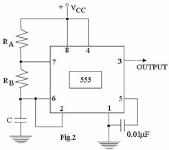
b. The IC555 timer is connected as shown in the Fig.2.
|
What is this mode of operation called? What is the frequency and the duty cycle of the output wave generated? Sketch the output waveform. (8)