Code: D-06 Subject: BASIC ELECTRONICS
Time: 3 Hours June 2006 Max. Marks: 100
NOTE: There are 9 Questions in all.
· Question 1 is compulsory and carries 20 marks. Answer to Q. 1. MUST BE WRITTEN IN THE SPACE PROVIDED FOR IT in the answer book supplied and nowhere else.
· Out of the remaining EIGHT Questions answer any FIVE Questions. Each question carries 16 marks.
· Any required data not explicitly given, may be suitably assumed and stated.
Q.1 Choose the correct or best alternative in the following: (2x10)
a. Which one of the following statements is not true?
(A) Capacitance is a measure of a capacitor’s capability to store charge.
(B) A capacitor offers high impedance to ac but very low impedance to
dc.
(C) A capacitor is also used as bypass capacitor.
(D) Capacitors are used to couple alternating voltages from one circuit to another and at the same time to block dc voltage from reaching the next circuit.
b. A voltage source having an open-circuit voltage of 100 V and
internal resistance of 50![]() is equivalent to a current source
is equivalent to a current source
(A)
2A in
parallel with 50![]() . (B)
2A with 50
. (B)
2A with 50![]() in series.
in series.
(C) 0.5A in parallel with 50![]() . (D)
2A in parallel with 100
. (D)
2A in parallel with 100![]() .
.
c. In a Zener diode large reverse current is due to
(A) collision. (B) presence of impurities.
(C) rupture of bonds (D) lower resistance in reverse biased
region.
d. Ripple factor of a full-wave rectifier without filter will be
(A) 0.2. (B) 0.48.
(C) 0.24. (D) 1.21.
e. JFET has main drawback of
(A) having low input impedance.
(B) having high output impedance.
(C) being noisy.
(D) Having small gain-bandwidth product.
f. A UJT has
(A) stable negative resistance characteristics.
(B) low firing current.
(C) use as a waveform generator.
(D) all of these characteristics.
g. For thermionic emission
(A) a material with high work function is preferable.
(B) a material with low work function is preferable.
(C) the work function of the material has no importance.
(D) None of these is true.
h. Ideal operational amplifier has input impedance of
(A)
![]() . (B)
infinity.
. (B)
infinity.
(C) zero. (D)
![]() .
.
i. The CE configuration amplifier circuits are preferred over CB configuration amplifier circuits because they have
(A) lower amplification factor.
(B) Larger amplification factor.
(C) high input resistance and low output resistance.
(D) none of these.
j. In a differential amplifier an ideal CMRR is
(A) infinity. (B) zero.
(C) –1. (D) +1.
Answer any FIVE Questions out of EIGHT Questions.
Each question carries 16 marks.
Q.2 a. What are active and passive components? Categorise the following components into these categories. Mettalized polyster capacitor, Preset Filter circuits, Audio-frequency chokes, FET, Vacuum tubes. (4+4)
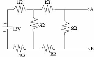
b. Determine Thevenin’s equivalent circuit which may be used to represent the given network at the terminals A-B. (8)
|
Q.3 a. Draw the energy band diagram of a P-N junction under open-circuited condition. Clearly indicate energy levels in P-region, space region and N-region. How will it be modified if P-N junction is forward biased? (8)
b. In an N-type semi
conductor, the Fermi-level lies 0.3 eV below the conduction band at ![]() . If the
temperature is increased to
. If the
temperature is increased to ![]() , find the new position of the
Fermi-level. (8)
, find the new position of the
Fermi-level. (8)
Q.4 a. Draw input and
output characteristics of common base transistor configuration. Derive
relation between ![]() and
and
![]() . (8)
. (8)
b. In a transistor circuit
load resistance is ![]() and quiescent current is 1.2 mA.
Determine the operating point when the battery voltage
and quiescent current is 1.2 mA.
Determine the operating point when the battery voltage ![]() . How will the Q-point
change when the load resistance is changed from
. How will the Q-point
change when the load resistance is changed from ![]() to
to ![]() ? (8)
? (8)
Q.5 a. Sketch and explain the basic structure of an N-channel junction field effect transistor. (8)
b. Why is a FET known as a unipolar device? How do you compare this device with BJT? (8)
Q.6 a. Explain the terms “work function” and “threshold frequency” in connection with electron emission. Name one material suitable for thermionic emission and one material for photo-emission. (8)
b. What are photoelectric emission? How is the electron emission affected if
(i) the frequency and
(ii) the intensity of the incident radiations are increased? (8)
Q.7 a. Explain the working of a full-wave rectifier using centre-tapped transformer. What is PIV of this rectifier? (8)
b. A half-wave rectifier
having a diode of resistance 1,000![]() and a load of 1,000
and a load of 1,000![]() rectifies an ac
voltage of 310 V peak value. Calculate
rectifies an ac
voltage of 310 V peak value. Calculate
(i) peake, average and rms values of current.
(ii) dc power output.
(iii) ac power input.
(iv) efficiency. (8)
Q.8 a. Draw the schematic diagram of an op-amp connected as
(i) an inverter (ii) a scale changer
(iii) a phase shifter and (iv) an adder. (8)
b. Implement
the following equation using two operational amplifiers ![]() . Use minimum value of
resistance as
. Use minimum value of
resistance as ![]() . (8)
. (8)
Q.9 a. Briefly explain the thin-film and thick –film methods of producing ICs. Discuss their advantages and limitations. (8)
b. Differentiate between SSI, MSI, LSI and VLSI. (8)