Code: C-03 / T-03 Subject: BASIC ELECTRONICS & DIGITAL CIRCUITS
Time: 3 Hours June 2006 Max. Marks: 100
NOTE: There are 9 Questions in all.
· Question 1 is compulsory and carries 20 marks. Answer to Q. 1. must be written in the space provided for it in the answer book supplied and nowhere else.
· Out of the remaining EIGHT Questions answer any FIVE Questions. Each question carries 16 marks.
· Any required data not explicitly given, may be suitably assumed and stated.
Q.1 Choose the correct or best alternative in the following: (2x10)
a. What is the effect of increase in reverse bias on a pn junction.
(A) The width of depletion layer is increased
(B) The width of depletion layer is decreased
(C) The concentration of majority carriers is increased
(D) None of the above
b. The input impedance of the following configuration of amplifier is very high
(A) Common base amplifier (B) Common emitter amplifier
(C) Common collector amplifier (D) None of the above
c. In the circuit shown in Fig.1
![]()
![]() . The
operating point
. The
operating point
![]() and
and ![]() are given by
are given by
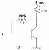
(A) 4.6V and 1.98 mA
(B) 4.7V and 2 mA
(C) 5.4V and 1.56 mA
(D) 4.2V and 2.1 mA
d. The reactance of 0.2 microfarad capacitor is equal to 1000 ohms at the frequency of
(A) 800 Hz (B) 1 kHz
(C) 1 MHz (D) 8 MHz
e. The function ![]() is an
example of a Boolean function expressed in
is an
example of a Boolean function expressed in
(A) K-map (B) POS form
(C) SOP form (D) Truth table
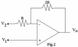
f. In the op
amp circuit shown in Fig.2 ![]() is given by
is given by
(A) 3V1 – 6V2 (B) 2V1 – 3V2
(C) 2V1 – 2V2 (D) 3V1 – 2V2
|
g. In the CMOS inverter the power dissipation is
(A) low only when input is low (B) low only when input is high
(C) high during dynamic operation (D) low during dynamic operation
h. The noise margin of TTL logic devices is of the order of
(A) 0.1 volts (B) 0.4 volts
(C) 5 volts (D) 0.7 volts
i. Which of the following circuits and is suitable for generating a signal of 1kHZ frequency.
(A) Wien bridge oscillator (B) tuned collector oscillator
(C) Hartley oscillator (D) Colpitts oscillator
j. Among the logic families the one having lowest power dissipation is
(A) TTL (B) ECL
(C) CMOS (D) DTL
Answer any FIVE Questions out of EIGHT Questions.
Each question carries 16 marks.
Q.2 a. Draw the characteristics of a zener diode and explain its operation. (5)
b. With the help of a circuit diagram, explain the use of a zener diode as a peak clipper. (5)
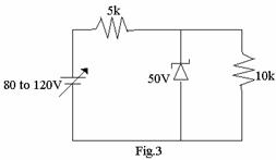
c. Find the maximum and minimum value of zener diode current and supply current in the circuit shown in Fig.3. Assume ideal zener diode. (6)
Q.3 a. Draw the circuit diagram of a single stage RC coupled amplifier. (4)
b. Draw the frequency response curve of a single stage RC coupled amplifier. (3)
c. What do you understand by the bandwidth of an amplifier? Explain with reference to an RC-coupled amplifier. (9)
Q.4 a. Draw the circuit diagram of RC phase
shift oscillator and derive the condition for oscillation. Neglect the effects
of ![]() . (12)
. (12)
b. A transistorized RC phase shift
oscillator uses three resistors of value R = 600 K ohms and three
capacitors of value C = 100 pico farads. The collector resistance is 300k
ohms. Calculate the frequency of oscillation and the minimum ![]() required for the transistor. (4)
required for the transistor. (4)
Q.5 a. Define and explain the terms input bias current, input offset voltage, open loop gain, CMRR and slew rate as applied to an operational amplifier. (8)
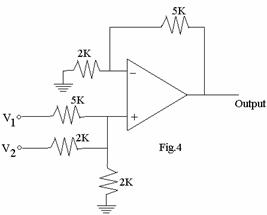
b. Find the output voltage of the following op amp circuit (Fig.4). (8)
|
Q.6 a. Draw the circuit diagram of a fullwave rectifier circuit with capacitor filter and explain its operation by drawing its output waveform. (10)
b. List three applications of ROM and explain them briefly. (6)
Q.7 a. An amplifier using BJT as a switch along with input voltage is shown in Fig.5. Draw the waveform of the output voltage and collector current showing the important features on the waveform. (12)
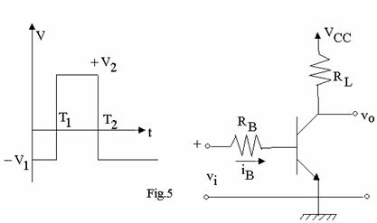
b. The circuit shown
uses ![]() ,
, ![]() ,
, ![]() , V2 = +5 volts
and V1 = -5 volts.
, V2 = +5 volts
and V1 = -5 volts. ![]() of the transistor used is 50. With
usual assumption calculate the important parameters of the waveform of part a
of the question. (4)
of the transistor used is 50. With
usual assumption calculate the important parameters of the waveform of part a
of the question. (4)
Q.8 a. Distinguish between synchronous and asynchronous counters. (4)
b. Draw the excitation table and truth table of JK flipflops. (4)
c. Write notes on charge coupled devices. (8)
Q.9 a. Explain the meaning of the terms noise margin, fan in and fan out as applied to logic gates with suitable examples. (9)
b. With the help of a truth table, design a full adder circuit using logic gates. Draw the circuit. (7)