Code: A-27 Subject: DIGITAL HARDWARE DESIGN
Time: 3 Hours June 2006 Max. Marks: 100
NOTE: There are 9 Questions in all.
· Question 1 is compulsory and carries 20 marks. Answer to Q. 1. must be written in the space provided for it in the answer book supplied and nowhere else.
· Out of the remaining EIGHT Questions answer any FIVE Questions. Each question carries 16 marks.
· Any required data not explicitly given, may be suitably assumed and stated.
Q.1 Choose the correct or best alternative in the following: (2x10)
a. Hamming code for LED-SEC has the following code received: 0110110. The corrected code is
(A) 0010110 (B) 0010110
(C) 1110110 (D) 0111110
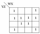
b. K-map for a switching function is shown below:
Identify which one of the following is true. The function has
(A) One essential and two non-essential prime implicants.
(B) Two essential and one non-essential prime implicants.
(C) Two essential and two non-essential prime implicants.
(D) Three essential prime implicants only.
c. In an FPLA
(A) Only AND arrays are programmable.
(B) Only OR arrays are programmable.
(C) Both the AND array and the OR array are programmable.
(D) None of these are programmable.
d. Simplifying
the following Boolean function ![]() gives
gives
(A)
![]() (B)
(B)
![]()
(C) ![]() (D)
(D) ![]()
e. A
function ![]() is
described by the expression z =
is
described by the expression z = ![]() . Applying Shannon’s decomposition with respect to
. Applying Shannon’s decomposition with respect to ![]() , we get
, we get
(A)
![]()
(B)
![]()
(C)
![]()
(D)
![]()
f. For a Moore canonical network, the input and output networks have a propagation delay of 2.5 ns and 3 ns respectively. The set up time of the register cells is 0.3 ns and the propagation delay is 1 ns. The network input stabilises no later than 2 ns after the triggering edge of the clock. The output needs to be stable for 3 ns before the next triggering edge. The maximum clock frequency for the above network approximately is
(A) 100 MHz (B) 120 MHz
(C) 50 MHz (D) 140 MHz
g. Identify one expression, which is not the characteristic expression of any flip-flop.
(A) Q (t+1) = D (t) (B) Q (t+1)= Q(t) R1(t) + S(t)
(C) Q (t+1) = Q(t) K1(t)+Q1(t) J(t) (D) Q (t+1)= Q(t) +T(t)
h. In VHDL, a configuration is needed to
(A) Bind architecture body to its entity declaration.
(B) Bind a component with an entity.
(C) Specify a top-level entity in terms of low level entities.
(D) All of the above.
i. The U and Z values in model simulation refer to
(A) User defined and high impedance values.
(B) Undefined and high impedance values.
(C) U and z formats.
(D) User and z models.
j. A postponed process means
(A) a process that executes only at the end of all deltas of the simulation time in which an event triggered the process to resume execution.
(B) A process that is postponed before a trigger process is initiated.
(C) A process that is postponed till the next process execution starts.
(D) A keyword for postponing the existing process.
Answer any FIVE Questions out of EIGHT Questions.
Each question carries 16 marks.
Q.2 a. Use the tabulation procedure to generate the set of prime implicants and to obtain all minimal expressions for the following function.
![]() (7)
(7)
b. Construct the decomposition chart for the function given below:
![]()
Indicate
all possible decompositions and determine specifically the functions F and ![]() such that
such that ![]() (4)
(4)
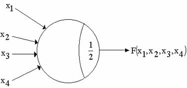
c. Find
the function of ![]() realised
by each of the threshold network shown in the following figure. Show the map of
each function. (5)
realised
by each of the threshold network shown in the following figure. Show the map of
each function. (5)
|
Q.3 a. Describe the high level description of (i) Priority encoder (ii) Shift register (iii) Counter. (8)
b. Determine a ROM and a PLA based implementation for the following system.
Input : a![]()
b ![]()
Output: ![]()
Function: 
Where a, b, z are the integers represented by the corresponding vectors in radix-2 number system. Note that –1 mod 8 is defined as 7. (8)
Q.4 a. Define pulse mode and fundamental mode in FSM. (5)
b. Design a sequential system with one binary input x and one binary output z. The output at time t is 1 whenever x(t-3, t) = 0101. Write the state table and draw the state diagram. (4)
c. For the following machine shown in Table 1, find the equivalence partition and a corresponding reduced machine in standard form. (7)
|
PS |
NS, Z |
|
x = 0 x =1 |
|
|
A |
D, 0 H, 1 |
|
B |
F, 1 C, 1 |
|
C |
D, 0 F, 1 |
|
D |
C, 0 E, 1 |
|
E |
C, 1 D, 1 |
|
F |
D, 1 D,1 |
|
G |
D, 1 C,1 |
|
H |
B, 1 A,1 |
Table 1
Q.5 a. For the incompletely specified machine shown below in Table 2, find a minimum state reduced machine containing the original one. (10)
|
PS |
NS, Z |
|
I1 I2 I3 |
|
|
A |
C,0 E,1 - |
|
B |
C,0 E,- - |
|
C |
B, - C,0 A,- |
|
D |
B, 0 C,- E,- |
|
E |
- E, 0 A,- |
Table 2
b. Distinguish between Mealy and Moore machines. (6)
Q.6 a. Generate an ASM chart for adding two unsigned 8-digit BCD numbers using array variables. (6)
b. Compare PROM, PAL and FPLA devices. (4)
c. Two 4 bit registers X and Y are loaded with values. On a start signal, X and Y are compared. If X>Y, flip flop A is set to 1. If X<Y, a flip flop B is set to 1. If X = Y, flip flop E is set to 1. It is needed to load X and Y and clear all flipflops and give a start signal. On start, the MSBs of X and Y (namely X3 and Y3) are compared. Write a ASM chart, state transition diagram and operations that take place during a clock interval. (6)
Q.7 a. A state transition diagram for a Moore finite state machine is shown below:
|
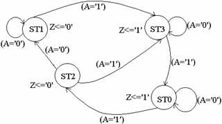
Write the behaviour model to implement the above, using a single process and case statement. (8)
b. Write the VHDL code for the following:
(i) 4:1 multiplexer.
(ii) D-Latch. (8)
Q.8 a. Determine which of the following functions is symmetric and identify its a-numbers and variables of symmetry.
(i) ![]()
(ii) ![]()
(iii)
![]() (10)
(10)
b. Write a note on computer aided design tools which you have studied. (6)
Q.9 a. Write explanatory notes on (Any FOUR)
(i) FPGA
(ii) Microinstruction sequencer.
(iii) Dataflow and structural style modelling in VHDL.
(iv) Hazards and races in ASM.
(v) Incompletely specified machines. (4 x 4 = 16)