Code: A-09 Subject: ANALOG & DIGITAL ELECTRONICS
Time: 3 Hours June 2006 Max. Marks: 100
NOTE: There are 9 Questions in all.
· Question 1 is compulsory and carries 20 marks. Answer to Q. 1. must be written in the space provided for it in the answer book supplied and nowhere else.
· Out of the remaining EIGHT Questions answer any FIVE Questions. Each question carries 16 marks.
· Any required data not explicitly given, may be suitably assumed and stated.
Q.1 Choose the correct or best alternative in the following: (2x10)
a. A second order filter has a transfer function
 the poles and
zeros of this filter are at
the poles and
zeros of this filter are at
(A)
![]() . (B)
. (B)
![]() .
.
(C)
![]() . (D)
. (D)
![]() .
.
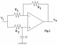
b. The circuit shown in Fig.1 represent a
(A) Low pass filter.
(B) High pass filter.
(C) Band pass filter.
(D) None of the above.
|
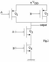
c. The circuit in Fig.2 is
used to realize the logic function of
(A) Inverter.
(B) NOR gate.
(C) NAND gate.
(D) XOR gate.
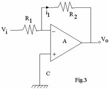
d. Consider an
inverting op amp circuit at Fig.3 with feedback resistor equal to 100 K![]() and the input
resistor equal to 1K
and the input
resistor equal to 1K![]() with a gain of 100 if the op amp has
infinite open loop gain. If the op amp has a finite open loop gain at
with a gain of 100 if the op amp has
infinite open loop gain. If the op amp has a finite open loop gain at ![]() ; the gain of the
op amp circuit is
; the gain of the
op amp circuit is
(A) 100. (B) 101.
(C) 98. (D) 99.
e. For standard TTL
logic circuits, the values of ![]() and
and ![]() are
are
(A) 0.8 V and 2.0 V. (B) 0 V and 5 V.
(C) 0.4 V and 2 V. (D) 0.4 V and 2.4 V.
|
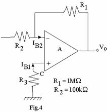
f. An op amp with input offset voltage
![]() is used in the
circuit shown
is used in the
circuit shown
in Fig.4. If the input bias currents
IB1 = IB2 = 100 nA then the value of
Resistance R3, such that the output
voltage is zero for zero input voltage, is
(A)
![]()
(B)
![]()
(C) ![]()
(D) ![]()
g. In a sample and hold circuit the following statement is false
(A) Sample time is much smaller than hold time.
(B) Aperture time is the delay between the time that the pulse is applied to the switch and the actual time the switch closes.
(C) Acquisition time is the time it takes for the capacitor to charge from one voltage to another voltage.
(D) The voltage across the hold capacitor changes by 50% during hold time.
h. The voltage between the emitter and collector of a silicon transistor when the transistor is biased to be at the edge of saturation is:
(A) 5 volts. (B) 10 volts.
(C) 0.1 volts. (D) 0.3 volts.
i. The fastest switching logic family is
(A) CMOS. (B) TTL.
(C) DTL. (D) ECL.
j. A 32 to 1 multiplexer has the following features.
(A) 32 outputs, one input and 5 control signals
(B) 32 inputs, one output and 5 control signals
(C) 5 inputs, one control signal and 32 outputs
(D) 5 inputs 32 control signals and one output
Answer any FIVE Questions out of EIGHT Questions.
Each question carries 16 marks.
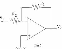
Q.2 a. Derive an equation for the closed loop gain of an operational amplifier circuit shown in Fig.5 if the open loop gain of the op amp is A. (4)
b. Explain the meaning of the terms slew rate, input offset voltage, input bias current and input offset current. (8)
c. Write briefly on instrumentation amplifier. (4)
Q.3 a. A
third order low pass filter has two transmission zeros at ![]() and at infinity. Its
natural modes are at
and at infinity. Its
natural modes are at ![]() and
and ![]() . Find the value of the transfer
function if the d.c. gain is 5. (6)
. Find the value of the transfer
function if the d.c. gain is 5. (6)
b. Plot the response of a typical low pass Butterworth filter and explain the response by identifying the different parameters. (5)
c. Sketch the transmission characteristics of an even and odd order Chebyshev low pass filter and identify the important parameters. (5)
Q.4 a. Describe the counting type analog to digital converter with the help of a block diagram. (12)
b. Explain the meaning of the terms conversion time and resolution of an analog to digital converter. (4)
Q.5 a. Explain the use of Schottky barrier diode in increasing the speed of switching. (4)
b. Explain the operation of BJT as a switch. (6)
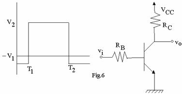
c. The voltage shown in Fig.6 on the left is in applied to the circuit on the right. Sketch the output voltage as a function of time and explain how you get that particular output. (6)
Q.6 a. Explain different TTL logic families and compare their performance. (4)
b. Draw a basic ECL logic NOR gate, and explain its operation. (12)
Q.7 a. Design a 1 bit digital comparator using basic logic gates to get three different outputs and draw the circuit diagram. Using this, design a four bit comparator. (12)
b. You are given two types demultiplexers of four output and eight outputs. Design a 32 output demultiplexer using these devices. (4)
Q.8 a. What do you understand by a race around condition? (2)
b. Draw the circuit diagram of master slave JK flipflop and explain its operation. (10)
c. Explain how do you measure the frequency using a counter. (4)
Q.9 a. Draw the diagram of a emitter coupled bipolar memory cell and explain its operation. (8)
b. Explain the operation of PROM, and EPROM. (8)