Code: A-05 June 2006 Subject: BASIC ELECTRONICS
Time: 3 Hours Max. Marks: 100
NOTE: There are 9 Questions in all.
· Question 1 is compulsory and carries 20 marks. Answer to Q. 1. must be written in the space provided for it in the answer book supplied and nowhere else.
· Out of the remaining EIGHT Questions answer any FIVE Questions. Each question carries 16 marks.
· Any required data not explicitly given, may be suitably assumed and stated.
Q.1 Choose the correct or best alternative in the following: (2x10)
a. The electron relaxation time
of metal A is ![]() ,
that of B is
,
that of B is ![]() .
The ratio of resistivity of B to resistivity of A will be
.
The ratio of resistivity of B to resistivity of A will be
(A) 4. (B) 2.0.
(C) 0.5. (D) 0.25.
b. The overall bandwidth of two identical voltage amplifiers connected in cascade will
(A) remain the same as that of a single stage.
(B) be worse than that of a single stage.
(C) be better than that of a single stage.
(D) be better if stage gain is low and worse if stage gain is high.
c. Field effect transistor has
(A) large input impedance. (B) large output impedance.
(C) large power gain. (D) large voltage gain.
d. Which of the following parameters is used for distinguishing between a small signal and a large-signal amplifier?
(A) Voltage gain (B) Frequency response
(C) Harmonic Distortion (D) Input/output impedances
e. Which of the following will not decrease as a result of introduction of negative feedback?
(A) Instability (B) Bandwith
(C) Overall gain (D) Distortion
f. If the feedback signal is returned to the input in series with the applied voltage, the input impedance _________.
(A) decreases (B) increases
(C) does not change (D) becomes infinity
g. Most of linear ICs are based on the two transistor differential amplifier because of its
(A) input voltage dependent linear transfer characteristic.
(B) high voltage gain.
(C) high input resistance.
(D) high CMRR
h. The waveform of the output voltage
for the circuit shown in the Fig.1 (RC>>1) is a
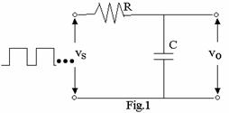
(A) sinusoidal wave. (B) square wave.
(C) series of spikes. (D) triangular wave.
i. A single phase diode bridge rectifier supplies a highly inductive load. The load current can be assumed to be ripple free. The ac supply side current waveform will be
(A) sinusoidal. (B) constant dc.
(C) square. (D) triangular.
j. Which of the following Boolean rules is correct?
(A) A+0 = 0 (B) A+1 = 1
(C) ![]() (D)
(D) ![]()
Answer any FIVE Questions out of EIGHT Questions.
Each question carries 16 marks.
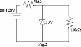
Q.2 a. State and explain the characteristics of a zener diode. How it can be used as a voltage regulator? (8)
b. For
the circuit shown in Fig.2, find the maximum and minimum values of zener diode
current. (8)
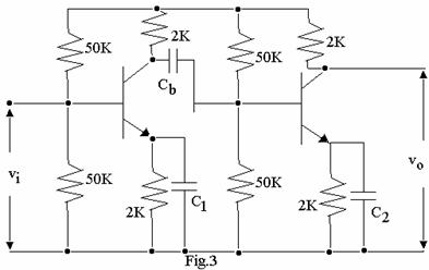
Q.3 a. What is a cascode pair? Give the basic circuit characteristic of a cascode amplifier. (8)
b. The parameters of the
transistor in the circuit shown in Fig.3 are ![]() . Find
. Find
(i) midband gain
(ii) the value of ![]() necessary to give
a lower 3 dB frequency of 20 Hz
necessary to give
a lower 3 dB frequency of 20 Hz
(iii) the value of ![]() necessary to ensure
less than 10% tilt for a 100 Hz square wave input. (8)
necessary to ensure
less than 10% tilt for a 100 Hz square wave input. (8)
|
Q.4 a. What are the relative merits and demerits of a FET amplifier over a transistor amplifier? (8)
b. Draw circuit of a transformer coupled single stage transistor power amplifier and explain the need for impedance matching. (8)
Q.5 a. Derive mathematical expressions showing how the application of negative feedback in amplifiers affects the following characteristics of the amplifier.
(i) Frequency response. (ii) Stability of gain. (8)
b. Draw a neat circuit diagram of a Colpitt’s oscillator using an N-P-N transistor. Give its equivalent circuit. Derive the expression for the following :
(i) the frequency of oscillations.
(ii) the minimum gain for sustained oscillations. (8)
Q.6 a. Explain the operation of an op-amp as a subtractor. (8)
b. For the circuit shown in Fig.4,
determine voltage gain, input impedance, output impedance, common-mode gain and
CMRR if
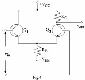
![]()
![]() and transistors
and transistors ![]() and
and ![]() are identical with
are identical with
![]() .
Determine output voltage when
.
Determine output voltage when ![]() and when
and when ![]() . (8)
. (8)
Q.7 a. Sketch the circuit of a Schmitt trigger and explain its operation. What is hysteresis? (8)
b. In an astable
multivibrator, the base resistors are of 12.5![]() and the capacitors are of 0.01
and the capacitors are of 0.01![]() . Determine the
PRR (Pulse Repetition Rate). (8)
. Determine the
PRR (Pulse Repetition Rate). (8)
Q.8 a. Draw the circuit diagram of a bridge rectifier and derive its ripple factor and efficiency with and without filter. (8)
b. A
single-phase full-wave rectifier uses two diodes, the internal resistance of
each being 20![]() .
The transformer rms secondary voltage from centre tap to each end of secondary
is 50V and load resistance is 980
.
The transformer rms secondary voltage from centre tap to each end of secondary
is 50V and load resistance is 980![]() . Find
. Find
(i) the mean load current
(ii) rms load current and output efficiency. (8)
Q.9 a. Show how Karnaugh map is used for minimisation of Boolean functions. (8)
b. Simplify the following expression using Boolean algebra technique
![]() (8)
(8)