DipIETE
– ET (NEW SCHEME) – Code: DE56
Subject: ANALOG ELECTRONICS
 Time: 3 Hours
Max. Marks: 100
Time: 3 Hours
Max. Marks: 100
NOTE: There are 9 Questions in all.
· Question 1 is compulsory and
carries 20 marks. Answer to Q. 1 must be written in the space provided for it
in the answer book supplied and nowhere else.
· Out of the remaining EIGHT
Questions answer any FIVE Questions. Each question carries 16 marks.
· Any required data not
explicitly given, may be suitably assumed and stated.
Q.1 Choose
the correct or the best alternative in the following: (2![]() 10)
10)
a. A Schmitt Trigger circuit can
be used as
(A) constant current source (B) differential amplifier
(C) series clipping circuit (D) fast-operating voltage level detector
b.
The ________________ is used for a low
voltage source to control high voltages, a switch and electric isolation
between input and output terminals.
(A) common emitter circuit (B) opto-coupler
(C) TRIAC (D) negative feedback amplifier
c. The practical
maximum efficiency for a class-A transformer coupled power amplifier is around
(A) 85% (B) 65%
(C) 50% (D) 25%
d. Coupling
capacitors in the input or the output of amplifiers are for
(A) offering dc and ac open-circuits
(B) coupling the signal in the circuit
(C) passing the output waveform to the load and changing the circuit bias condition
(D) altering the circuit bias at the input of the circuit
e. Which is the fastest ADC?
(A) parallel comparator (B) dual slope converter
(C) successive approximation type (D) integrating type
f. Practical IC op-amps have slew rates of the order of
(A) 1mV/us to 10mV/us (B) 1mV/us to 100 mV/us
(C) 100 mV/us to above 1000 V/us (D)
0.1 uV/us to 0.2 uV/us
g. The slew rate____________
(A) is a small-signal phenomenon
(B) if its value is exceeded, results in distortion
(C) is the minimum time rate of change of the output voltage
(D) its limiting depends on only the power supply voltage
h. Number of
components on the chip in a VLSI package are up to around
(A) 1,00 (B)
5,00
(C) 1,000 (D) 10,000
i. A 555 IC timer can produce
(A) very accurate and unstable time delays
(B) not so accurate time delays and unstable
(C) very accurate and stable time delays
(D) none of the above
j. In an IC
monolithic transistor, the collector contact is
(A) on top of the subtract (B) on top or bottom of the
subtract
(C) on either sides of the subtract (D) on bottom of the subtract
Answer any FIVE Questions out
of EIGHT Questions.
Each question carries 16
marks.
Q.2 a. Compare
the performance of CE, CB, and CC circuits.
Discuss typical applications of each type of circuit. (10)
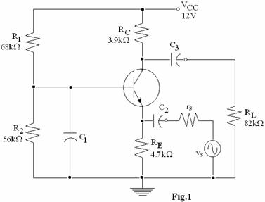
b. The transistor in the CB circuit in Fig. 1 has the
following parameters:
hie =
2.1 k![]() and
hfe =75. Calculate the circuit input and output impedances and
voltage gain. (2+2+2)
and
hfe =75. Calculate the circuit input and output impedances and
voltage gain. (2+2+2)
Q.3 Describe briefly the fabrication processes and
technology for monolithic IC, typical circuits for active and passive
components, thin and thick film devices. (6+6+4)
Q.4 a. Explain working of a junction field effect
transistor (JFET). (8)
b. With neat diagrams, describe n-channel JFET and
p-channel JFET. Give their circuit symbols. (6+2)
Q.5 a. Explain
working principle of class - A, class - B and class - AB transformer coupled
audio power amplifiers. Give their diagrams. (8)
b. Derive expression for the efficiency of a class - A
amplifier. What is the maximum theoretical efficiency and typical practical
maximum efficiency for a class - A transformer coupled power amplifiers? (6+2)
Q.6 a. Give circuit diagrams for op-amp based
direct-coupled and capacitor-coupled inverting and non-inverting amplifiers;
and briefly give their salient features. (4+4)
b. Explain in brief DC and AC characteristics of an op-amp. (8)
Q.7 a. Explain sample and hold circuit using op-amp. (8)
b. Draw
circuit diagram of a typical OP-Amp based Instrumentation Amplifier. Briefly
discuss its properties in respect of output and common mode rejection. (6+2)
Q.8 a. What are the basic DAC techniques? With a schematic
diagram, mathematically describe functioning of a voltage output D/A converter. (8)
b. What
output voltage would be produced by a D/A converter whose output range is 0 to
10 V and whose input binary number is 10 (for a 2-bit DAC), 0110 (for a 4-bit
DAC) and 10111100 (for a 8-bit DAC). (8)
Q.9 Write brief notes on:
(i) Schmitt
Trigger.
(ii) Monostable
and Astable operations.
(8 ![]() 2 = 16)
2 = 16)