DipIETE
– CS (OLD SCHEME)
Code: DC02 Subject: FUNDAMENTALS OF ELECTRONICS
 Time: 3 Hours
Max. Marks: 100
Time: 3 Hours
Max. Marks: 100
NOTE: There are 9 Questions in all.
· Question 1 is compulsory and
carries 20 marks. Answer to Q.1 must be written in the space provided for it in
the answer book supplied and nowhere else.
· Out of the remaining EIGHT
Questions answer any FIVE Questions. Each question carries 16 marks.
· Any required data not
explicitly given, may be suitably assumed and stated.
Q.1 Choose
the correct or the best alternative in the following: (2![]() 10)
10)
a. If the colour code on the body
of the resistor given is green, blue and orange with no colour band for the
tolerance value, then the value of the resistance is
(A) ![]()
![]() 10% (B)
10% (B) ![]()
![]() 10%
10%
(C) ![]()
![]() 20%. (D)
20%. (D) ![]()
![]() 5%
5%
b. A constant-current source has
(A)
zero
internal resistance (B)
high internal resistance
(C) approximately zero resistance (D) infinite internal resistance
c. The donor type impurities
(A) create excess holes
(B) can be added to germanium but
not to silicon
(C) must have only five valance
electrons
(D) must have only three valance
electrons
d. The life time of typical ![]() is
is
(A)
100
hours (B) 300
hours
(C) 100,000+ hours (D) 10000 hours
e. A transistor is connected in C-E
configuration. If alpha for the
transistor is 0.996, than the collector current with no base current and an ![]() of one microampere
will be
of one microampere
will be
(A) ![]() (B)
(B)
![]()
(C) 25mA (D)
2 mA
f. The voltage gain of an amplifier without feedback is 400. With negative feedback introduced for the above amplifier, its gain for a feedback factor of 0.1 will be
(A)
1 (B) 8.5
(C) 9.76 (D) 5.25
g. The Boolean expression Y for the logic circuit shown in Fig.1 below is
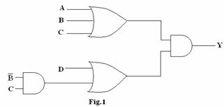
(A)
![]()
(B) ![]()
(C) ![]()
(D)
![]()
h. A TTL logic gate draws 2mA when its output is HIGH and 3.5 mA when its output is LOW. If the supply voltage is 5V, than the average power dissipation for the gate is
(A) 9.5 W (B) 13.7 mW
(C) 13.7![]() (D) 12.5 pw
(D) 12.5 pw
i. An ideal OPAMP has
(A) infinite ![]() (B)
infinite
(B)
infinite ![]()
(C)
zero ![]() (D)
all the above features
(D)
all the above features
j Integrated circuits are generally made of
(A) Germanium (B) Indium
(C) Gallium (D)
Silicon
Answer any FIVE Questions out
of EIGHT Questions.
Each question carries 16
marks.
Q.2 a. Which are the most commonly used passive
circuit components? Write three points
on each one of them. (1+9)
b. A dc voltage
source generating 500 V has an internal resistance of ![]() . Find the load
current if the load resistance is
. Find the load
current if the load resistance is
(i) ![]() (ii)
(ii) ![]() (6)
(6)
Q.3 a. Give the definition of a semiconductor in
terms of energy bands. Write the energy
band diagram for an intrinsic semiconductor. (5)
b. What is a PN junction? Define the quantity static forward resistance for a PN-junction. Explain how this quantity can be obtained using the V-I characteristics for the junction. What do you mean by static reverse resistance of the junction? (7)
c. Suggest ‘FOUR’
applications for a PN-junction. (4)
Q.4 a. Write the graphic symbols for the
conventional semiconductor diode and the Zener-diode indicating the conduction
direction. Comment on the complete
equivalent circuit of the Zener diode in the Zener region and the approximate
equivalent circuit. (6)
b. Define the term “electro luminescence”. Illustrate the process of electroluminescence
in the LED by a neat sketch, write the graphic symbol for an LED. (4)
c. Write a note
on varactor diodes. (6)
Q.5 a. Explain the basic operation of a BJT using a PNP transistor for illustration. (9)
b. Write the equation for the collector current
of a transistor in terms of ![]() and
and ![]() with usual
notations. Comment on the magnitude of the
collector current as per the above equation when the transistor is at cut-off
and when the transistor is in the active region. (5)
with usual
notations. Comment on the magnitude of the
collector current as per the above equation when the transistor is at cut-off
and when the transistor is in the active region. (5)
c. Rearrange the collector current equation of part (b) to write the collector current equation for a Common-Emitter transistor circuit. (2)
Q.6 a. What are the improvements obtained in an
amplifier with negative feedback introduced?
Write the schematic of a current-shunt feedback amplifier. (8)
b. An amplifier has a voltage gain of 1000. With negative feedback, if the voltage gain
reduces to 10 what is the fraction of the output that is fed back to the
amplifier’s input?
(3)
c. The specifications of a certain enhancement-type MOSFET are:
![]()
Is
this a P-channel or an N-channel device?
Compute the value of the drain current when ![]() . (5)
. (5)
Q.7 a. Write the following laws of Boolean algebra
and mention their use:
(i) Commutative laws. (ii) Distributive Laws. (6)
b. Write the circuit symbol and the truth table for the following logic gates
(i) A 3-input OR gate
(ii) Exclusive OR gate (6)
c. Write the procedure to convert a
non-standard SOP Boolean expression into a standard SOP form. Convert the Boolean expression ![]() to a standard SOP
form. (4)
to a standard SOP
form. (4)
Q.8 a. What is the advantage of Karnaugh map? A Karnaugh map is shown below. Write the logical equation in the standard
SOP form. (5)
|
|
00 |
01 |
11 |
10 |
|
00 |
1 |
|
1 |
|
|
01 |
|
1 |
|
1 |
|
11 |
|
1 |
1 |
|
|
10 |
|
|
1 |
|
AB
![]()
CD
b. A four-variable logic function is given by, ![]()
Minimise
the above function using K-map. Indicate
the minimisation steps. (7)
c. Name
the different transistor logic families that you are aware of. Distinguish between saturated and non
saturated logic circuits. (4)
Q.9 a. Why
are MOSFETS popular in logic circuits fabrication? Distinguish between PMOS and NMOS logic
circuits. What is the advantage of CMOS
logic? Write the circuit of a MOS
inverter with enhancement load. (7)
b.
Why OPAMPS have become popular in
electronic system design? When do you
say that an OPAMP is in open-loop condition?
Write the circuit of the basic non-inverting amplifier and the equation
for its voltage gain. (5)
c. Indicate two advantages and two disadvantages
of monolithic integrated circuits. (4)