AMIETE
– ET/CS/IT (NEW SCHEME) - Code: AE54/AC54/AT54
Subject: LINEAR ICs & DIGITAL ELECTRONICS
 Time: 3 Hours
Max. Marks: 100
Time: 3 Hours
Max. Marks: 100
NOTE: There are 9 Questions in all.
· Question 1 is compulsory and
carries 20 marks. Answer to Q. 1 must be written in the space provided for it
in the answer book supplied and nowhere else.
· Out of the remaining EIGHT
Questions answer any FIVE Questions. Each question carries 16 marks.
· Any required data not
explicitly given, may be suitably assumed and stated.
Q.1 Choose
the correct or the best alternative in the following: (2![]() 10)
10)
a. An op-amp has common mode gain of 50 dB and
its CMRR is 150 dB. The differential gain of it will be__________
(A) 7500 dB (B) 200 dB
(C) 100 dB (D) 3 dB
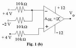
b.
The output voltage Vo in the given op-amp circuit as shown in Fig. 1
(b) is
(A) – 10 V (B) + 6 V
(C) + 8 V (D) + 10 V
c. Schmitt trigger
is also called as____________
(A) Astable Multivibrator. (B) Monostable Multivibrator
(C) Bistable Multivibrator (D) Square wave Generator
d. The main advantage in using a three op-amp
instrumentation amplifier over a single op-amp difference amplifier lies in
(A) Higher value of CMRR
(B) Lower noise Figure
(C) Elimination of the need for
accurate matching of resistors
(D) Simplicity of gain adjustment
e. The output voltage of the op-amp as shown in
Fig. 1(e), will be
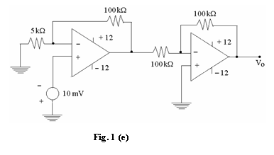
(A) – 210 mV (B) 200 mV
(C) – 200 mV (D) + 210 mV
f. The number of bytes in a 32-bit string is
(A) 2 (B) 4
(C) 6 (D) 8
g.
According to Demorgan’s Second theorem _________
(A) A NAND gate is always complementary
to an AND gate
(B) An AND gate is equivalent to a
bubbled NAND gate
(C) A NAND gate is equivalent to a
bubbled AND gate
(D) A NAND gate is equivalent to
a bubbled OR gate
h. An EX-OR gate produces high output only when two inputs are
(A) High (B) Low
(C) Different (D) Equal
i. A square wave with a period of 10 ![]() drives a T-flip flop. The period of the output signal will be
drives a T-flip flop. The period of the output signal will be
(A) 100 ![]() (B) 20
(B) 20 ![]()
(C) 10 ![]() (D) 5
(D) 5 ![]()
j. The factors to be considered in the design
and application of Successive-approximation
ADC’s are
(A) Stability and regulation of the
reference voltage source
(B) Overload and recovery
characteristics of the comparator
(C) Characteristics of analog switches
speed and response of the ladder network
(D) All the above
Answer any FIVE Questions out
of EIGHT Questions.
Each question carries 16
marks.
Q.2 a. List six characteristics of an ideal op-amp. (3)
b. Obtain closed
loop gain of practical Non-Inverting operational amplifier. (7)
c. In Non-Inverting
amplifier, the input voltage Vin = 0.6 V, feed back resistor
Rf
= 10 k![]() , R1 = 2.2 k
, R1 = 2.2 k![]() , load resistor connected at output with respect to
, load resistor connected at output with respect to
ground
is 1 k![]() . Calculate (i) closed loop gain (ii) output voltage (iii) load current (iv) output current Io flowing
from the output terminal of the op-amp.
. Calculate (i) closed loop gain (ii) output voltage (iii) load current (iv) output current Io flowing
from the output terminal of the op-amp.
(6)
Q.3 a. Draw and
explain the compensating circuit
(a) for input offset voltage
(b)
Bias current in op-amp inverting
amplifier (6)
b. With neat circuit diagram, explain the
working of three op-amp Instrumentation amplifier. (6)
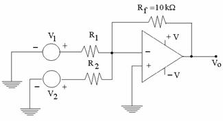
c. In inverting summing amplifier shown in Fig. 3
(c) below, solve for R1 and R2 if output voltage Vo
is average of two inputs V1 and V2. (4)
Fig. 3 (c)
Q.4 a. Draw sample and
hold circuit. Explain its operation and
indicate its uses. (6)
b. Design practical op-amp differentiator that
will differentiate an input signal with fmax = 500 Hz. (5)
c. Design Schmitt Trigger circuit for the
following specifications:
![]() = +3 V,
= +3 V, ![]() = + 1 V, Vsat
=
= + 1 V, Vsat
= ![]() 10 V. (5)
10 V. (5)
Q.5 a. With neat circuit diagram and waveform,
explain the working of op-amp as a Astable Multivibrator and show that T = 2 RC
ln ![]() . (8)
. (8)
b. With neat circuit
diagram, explain the 3-bit DAC (R-2R Ladder DAC). (5)
c. Design the values of R and C in Monostable Multivibrator
using 555 timer, so that output remains in high state for 0.5 m seconds. (3)
Q.6 a. Explain
functional diagram of Digital Computer. (6)
b. What
is parity bit? Explain Even parity and Odd parity method for Error detection. Why can’t the parity method detect
a double error in transmitted data? (4)
c. Perform the following conversions:
(i) (5467)10![]() (?)16 (ii) (6327.45)8
(?)16 (ii) (6327.45)8![]() (?)10
(iii) (3FC.82)16
(?)10
(iii) (3FC.82)16![]() (?)8 (6)
(?)8 (6)
(iv) (865)10![]() (?)BCD
(v) (47)16
(?)BCD
(v) (47)16![]() (?)ASCII (vi) (10101.011)2
(?)ASCII (vi) (10101.011)2![]() (?)10
(?)10
Q.7 a. Implement ‘OR’ logic using universal NAND
gate. (4)
b. Simplify the
following expression using K-map.
fABCD = ![]() +
+ ![]() +
+ ![]() + A (6)
+ A (6)
c. (i)
Simplify the following Boolean expression using postulates.
f = ![]() (3)
(3)
(ii) Determine the
input conditions needed to produce X = 1
in the Fig. 7(c) shown below (3)
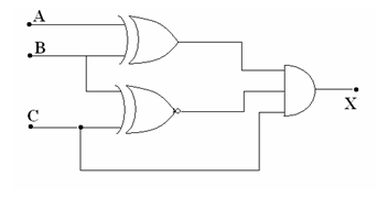
Fig. 7 (c)
Q.8 a. Design
a Full adder and implement it using EX-OR gates and Basic gates. (6)
b. What is
Multiplexer? Design four to one line MUX. (5)
c. Explain four bit IC 74LS85 Magnitude Comparator. (5)
Q.9 a. Explain the operation of NOR gate latch. (4)
b. With neat
Block diagram and sequence-table, explain working of Ring
Counter. (6)
c. Explain 4-bit Binary Asynchronous (ripple)
counter. (6)