AMIETE
– ET/CS/IT (NEW SCHEME) – Code: AE53/AC53/AT53
Subject: ELECTRONIC DEVICES AND CIRCUITS
 Time: 3 Hours
Max. Marks: 100
Time: 3 Hours
Max. Marks: 100
NOTE: There are 9 Questions in all.
· Question 1 is compulsory and
carries 20 marks. Answer to Q.1 must be written in the space provided for it in
the answer book supplied and nowhere else.
· Out of the remaining EIGHT
Questions answer any FIVE Questions. Each question carries 16 marks.
· Any required data not
explicitly given, may be suitably assumed and stated.
Q.1 Choose
the correct or the best alternative in the following: (2![]() 10)
10)
a. In practical current source, the source
impedance is
(A) zero
(B) very
low in comparison to load-resistance
(C) very high
in comparison to load-resistance
(D) infinite
b. Avalanche breakdown primarily depends on the
phenomenon of
(A) ionization (B) doping
(C) recombination (D) collision
c. For a given
emitter-current, the collector current can be increased by
(A) reducing
the recombination rate in the base region.
(B) doping
the emitter region lightly.
(C) reducing
the minority carrier mobility in the base region.
(D) making
the base region more wider.
d. If ![]() and
and ![]() for a transistor then
the value of
for a transistor then
the value of ![]() will be
will be
(A) 2.3 mA (B) 3.1 mA
(C) 4.6 mA (D) 5.2 mA
e. A FET
(A) incorporates
a forward bias junction.
(B) uses
a high concentration emitter junction.
(C) depends
on variation of a magnetic field for its operation.
(D) depends on the
variation of the depletion layer width with reverse voltage for its operation.
f. The
h-parameters are called hybrid-parameters because
(A) they are
obtained from different characteristics.
(B) they
have mixed dimensions.
(C) they are
mixed with other parameters.
(D) all
of the above.
g.
Multistage amplifiers are employed for having larger
(A) voltage
gain (B) power
gain
(C) frequency
response (D) all the
above
h. Transformer
coupling is used in a class A power amplifier, so as to make it
(A) More efficient (B)
less bulky
(C) less
costly (D) distortion
free
i. Feedback in an amplifier increases the input
impedance from ![]() to
to ![]() because of
because of
(A) positive
feedback (B) shunt-current
negative feedback
(C) series-current
negative feedback (D) shunt-voltage
negative feedback
j. In a RC-phase shift oscillator having three
stages, which have equivalent resistors and capacitors, in order to satisfy
Barkhausen criteria, should have a minimum gain of
(A) 6 (B) 29
(C) 31 (D) 49
Answer any FIVE Questions out
of EIGHT Questions.
Each question carries 16
marks.
Q.2 a. Obtain the response for a step input applied
to RC low pass circuit. (4)
b. State and
prove reciprocity theorem. (6)
c. For the resistive circuit shown in the Fig.
2c, find voltage V across the 40![]() resistance using mesh analysis. (6)
resistance using mesh analysis. (6)
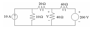
Fig. 2c
Q.3 a. Draw
Volt-Ampere characteristics of silicon p-n junction (4)
b. Define Transition and Diffusion capacitance. (4)
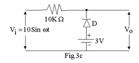
c. (i)
Draw the output waveform for the circuit shown in Fig.3c, considering Si
practical diode, assuming negligible Rf and infinite reverse
resistance (![]() ). (4)
). (4)
(ii) Show
that efficiency of the full-wave rectifier is
where Rs is Transformer secondary resistance.
Rf is forward diode drop
RL
is load resistance (4)
Q.4 a. Explain
two-Transistor model of SCR. (5)
b. With neat
diagram explain the Drain and Transfer characteristics of JFET. (6)
c. Define the current gain in Common Base and
Common Emitter configuration. Obtain the relation between them. (5)
Q.5 a. Explain the working of CMOS digital Inverter. (4)
b. A transistor as a Common-Emitter amplifier is
driving a load of 10 K![]() . It is supplied by a source of 1 K
. It is supplied by a source of 1 K![]() internal resistance. The hybrid parameters of the transistor
used are hie = 1.1 K
internal resistance. The hybrid parameters of the transistor
used are hie = 1.1 K![]() , hfe =50, hre=2.5
, hfe =50, hre=2.5 ![]() 10-4, hoe=
10-4, hoe=![]() .
.
Find
(i) current gain (ii)
Voltage gain (iii) Input impedance (iv)
Output impedance.
(6)
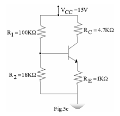 c. Find the
operating point for the circuit shown in Fig.5c, with
c. Find the
operating point for the circuit shown in Fig.5c, with ![]() =80 and VBE=0.6 V. Plot the DC load line and mark
Q-point. (6)
=80 and VBE=0.6 V. Plot the DC load line and mark
Q-point. (6)
Q.6 a. Mention
different types of distortion in Amplifiers. (3)
b. Obtain high frequency response of BJT
RC-Coupled amplifier. (7)
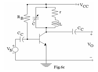
c. A 1mH
coil with Q=82 is used in tuned amplifier as shown in the Fig.6c. The
transistor employed has ![]() =125 and ro= 100 K
=125 and ro= 100 K![]() and input resistance
and input resistance
Ri = ![]() . (i) Calculate the
value of tuning capacitance such that the amplifier has a maximum gain at fo=45
kHz. Also calculate the value of this gain
(ii) Determine the bandwidth of the amplifier. (6)
. (i) Calculate the
value of tuning capacitance such that the amplifier has a maximum gain at fo=45
kHz. Also calculate the value of this gain
(ii) Determine the bandwidth of the amplifier. (6)
Q.7
a. With neat circuit diagram explain class-B Transformer coupled
Push-Pull power amplifier, show that maximum efficiency is 78.54%. (6)
b. What is
Cross-Over distortion? How do you eliminate it?
(4)
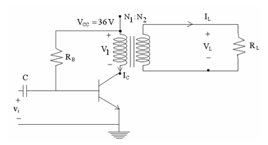 c. A transformer-coupled class-A
power amplifier as shown in Fig. 7c, drives a 16
c. A transformer-coupled class-A
power amplifier as shown in Fig. 7c, drives a 16 ![]() loud speaker through a
4:1 transformer with Vcc = 36 V, the circuit delivers 2W power to the load.
Find (i) power across the transformer primary
(ii) rms voltage across the load
(iii) rms voltage across the
transformer primary (iv) rms values of load current and primary
current (v) Conversion efficiency if the dc collector
current is 150 mA. (6)
loud speaker through a
4:1 transformer with Vcc = 36 V, the circuit delivers 2W power to the load.
Find (i) power across the transformer primary
(ii) rms voltage across the load
(iii) rms voltage across the
transformer primary (iv) rms values of load current and primary
current (v) Conversion efficiency if the dc collector
current is 150 mA. (6)
![]()
Q.8 a. What
are the properties of the negative feedback? (6)
b. Draw neat
circuit diagram of Wein-bridge Oscillator and show that resonant frequency fo=![]() . (6)
. (6)
c. Calculate the frequency of oscillations for
the BJT Hartley Oscillator given L1=750 ![]() H,
H, ![]() mutual inductance M=180
mutual inductance M=180 ![]() H and capacitance C=160 pF. (4)
H and capacitance C=160 pF. (4)
Q.9 a. Describe photolithographic process in IC
fabrication. (7)
b. Draw the cross-sectional view of Monolithic
n-p-n transistor and Discrete transistor. Compare the two types (6)
c. Calculate the chip area needed for a 220 pF
MOS capacitor, if the thickness of SiO2 layer is 480 Å and its relative dielectric
constant is 3.8. (3)