AMIETE – ET (OLD SCHEME)
Code: AE09 Subject: ANALOG & DIGITAL ELECTRONICS
 Time: 3 Hours
Max. Marks: 100
Time: 3 Hours
Max. Marks: 100
NOTE: There are 9 Questions in all.
· Question 1 is compulsory and
carries 20 marks. Answer to Q. 1. must be written in the space provided for it
in the answer book supplied and nowhere else.
· Out of the remaining EIGHT
Questions answer any FIVE Questions. Each question carries 16 marks.
· Any required data not
explicitly given, may be suitably assumed and stated.
Q.1 Choose the correct or the best
alternative in the following: (2x10)
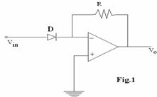
a. The circuit shown in Fig.1 is
(A) Logarithmic Amplifier.
(B)
Anti-logarithmic Amplifier.
(C) Clipper.
(D) Clamper.
b. In the differentiating circuit given in Fig.2,
the function of
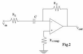
![]() is to
is to
(A) enable the circuit to approach
ideal differentiator
(B) maintain high input impedance
(C) eliminate high frequency noise spikes
(D) prevent oscillations at high frequencies
c. Digital ICs do not use
(A) P-channel MOSFETs (B) N-channel MOSFETs
(C) JFETs (D) N-P-N transistors
d. The number of flip flops required in a decade counter is
(A)
2 (B) 3
(C) 4 (D) 10
e. The number of comparisons carried out in a 4-bit flash-type A/D converter is
(A) 16 (B) 4
(C) 15 (D) 3
f. The primary switching delay in an over driven BJT is contributed by which one of the following characteristics of the transistor?
(A) Storage time (B)
Fall time
(C) Rise time (D) Charging time
g. For the circuit shown below in Fig.3, output F is
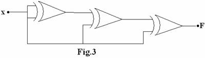
(A) F = 1
(B) F = x
(C) F = 0
(D) ![]()
h. The basic memory cell of dynamic RAM consists of
(A) a capacitance (B)
a transistor
(C) a flip flop (D) a transistor acting as a capacitor
i. Which one of the following is equivalent to AND-OR realization?
(A)
NAND-NOR
realization (B)
NOR-NOR realization
(C) NOR-NAND realization (D) NAND-NAND
realization
j. A PLA can be used
(A) as a microprocessor. (B) as a dynamic memory.
(C)
to realize a
sequential logic. (D) to realize a combinational logic.
Answer any FIVE Questions out
of EIGHT Questions.
Each question carries 16
marks.
Q.2 a. Discuss briefly how op-amp can be used as
instrumentation amplifier. (8)
b. Explain
following dc imperfections present in op-amps and how they are overcome?
(i)
Offset
voltage
(ii)
Input
bias currents. (8)
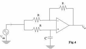
Q.3 a. Identify the filter and determine its
transfer function. (8)
b. Explain the working of second-order resonator. Discuss the two possible ways of exciting this resonator? (8)
Q.4 a. Draw the block diagram of a counting A/D
converter. Explain its operation. (8)
b. An 8 bit successive approximation A/D
converter has a resolution of 10mV. If
analog input is 1.592 V, find the digital output of ADC. (8)
Q.5 a. Explain
the advantage of using Schottky transistors in a TTL gate with totem pole
output. Draw the circuit of two input
Schottky TTL and explain its features. (8)
b. Describe following terms with respect to logic circuits
(i) Noise Margin
(ii) Propagation delay
(iii) Fan out
(iv)
Power delay product (8)
Q.6 a. Explain the operation of Dynamic RAM. Compare its advantages with respect to static
RAM. (8)
b. For each
statement indicate whether it pertains to MUX, DEMUX, ENCODER or DECODER
(i) can be
used to steer an input signal to one of several possible outputs.
(ii) produces a binary code at output.
(iii) was
select inputs.
(iv) has more
inputs than outputs.
(v) can be used as a logic function generator.
(vi) can
be used for parallel to serial conversion.
(vii) only
one of its outputs can be achieved at one time.
(viii) can be
used for data routing. (8)
Q.7 a. What is meant by the term edge-triggered flip
flop? Draw the circuit / block diagram
of positive edge triggered and negative edge triggered flip flop. (8)
b. What is a ring counter? How it is different from Johnson counter. (8)
Q.8 a. Explain following terms briefly w.r.t.
semiconductor memories:
(i) Memory cell (ii) Memory capacity
(iii) Access time (iv) Dynamic memory
(v) Read operation (vi)
Write operation
(vii) Erasable memory (viii) Static memory (8)
b. What is
interfacing? How interfacing is done
between TTL and ECL family? (8)
Q.9 Write short notes on the following:
(i)
4 bit
binary adder and subtractor.
(ii) CMOS
logic circuit.
(iii)
Transmission gates.
(iv)
NMOS-AND and NOR gates. (4x4 =16)