AMIETE – ET (OLD SCHEME)
 Code: AE05 Subject:
BASIC ELECTRONICS
Time: 3 Hours Max. Marks: 100
NOTE: There are 9 Questions in all.
· Question 1 is compulsory and
carries 20 marks. Answer to Q. 1. must be written in the space provided for it
in the answer book supplied and nowhere else.
· Out of the remaining EIGHT
Questions answer any FIVE Questions. Each question carries 16 marks.
· Any required data not explicitly
given, may be suitably assumed and stated.
Q.1 Choose
the correct or the best alternative in the following: (2x10)
a. With increasing temperature,
the resistivity of an intrinsic semiconductor decreases. This is because, with
the increase of temperature
(A) both the carrier concentration and
mobility of carriers decreases.
(B) the carrier concentration increases but
the mobility of carriers decreases.
(C) the
carrier concentration decreases but the mobility of carriers increases.
(D) the carrier concentration remains the same but the mobility of
carriers decreases.
b. RC coupling is popular in low-level audio amplifiers because it
(A)
has
better low frequency response.
(B)
is
inexpensive and needs no adjustments.
(C) provides an output signal in phase with the
input signal.
(D) needs low voltage battery for
collector supply.
c. The voltage gain of a given common-source JFET amplifier depends on its
(A) Input impedance. (B) Amplification factor.
(C) Dynamic drain resistance. (D) Drain load resistance.
d. The main function of a transformer employed at the output of a Power Amplifier is
(A)
to increase the voltage gain.
(B)
to step up the voltage and power.
(C) to match the load impedance with the dynamic
output impedance of transistor for maximum power transfer.
(D) to safeguard the transistor against
overheating.
e. The input impedance of an amplifier can be
increased from 2K![]() to 50 K
to 50 K![]() by introducing
by introducing
(A) Current-Shunt negative feedback.
(B) Voltage-Shunt negative
feedback.
(C) Current-Series negative feedback.
(D) Positive feedback.
f. An Oscillator which employs both Positive and Negative feedback is
(A) Hartley oscillator. (B) Colpitts oscillator.
(C) R-C Phase-Shift oscillator. (D) Wein-Bridge oscillator

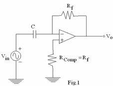
g. The OP-AMP circuit shown in Fig.1 is
(A) Comparator.
(B) Integrator.
(C) Differentiator.
(D) Summer.
h. A Schmitt Trigger is basically
(A) an Astable Multivibrator. (B) a Monostable
Multivibrator.
(C) a Bistable Multivibrator. (D) an Oscillator..
i. The output of Logic Gate is 1 when all its inputs are at Logic 0. The Gate is either
(A) a NAND or an EX-OR. (B) an OR or an EX-NOR.
(C) an AND or an EX-OR. (D)
a NOR or an EX-NOR.
j. A Ring counter consisting of five Flip-Flops will have
(A) 5 states. (B) 10 states.
(C) 32 states. (D) Infinite states.
Answer any FIVE Questions out
of EIGHT Questions.
Each question carries 16
marks.
Q.2 a. With neat diagrams, explain clearly why a
Common-Base connected Transistor
can exhibit Transistor action with the Collector-Base Junction voltage
reduced to zero.
(8)
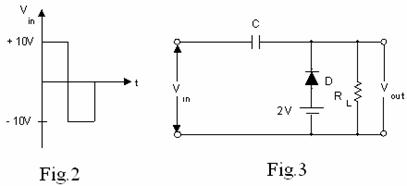
b. A Square wave shown in Fig.2 is applied to the circuit in Fig.3.
Name the circuit and explain its working. Sketch the output waveform. (8)

Q.3 a. Why are the h-parameters preferred to analyse
a circuit using Bipolar Transistor? Draw the h-Parameter equivalent circuit of
a CB transistor amplifier and derive an expression of (i) its Voltage Gain and
(ii) Current Gain. (10)
b. A 3-stage Cascaded Amplifier has voltage gains of 40, 60 and 80 respectively.
(i) Calculate the overall voltage gain in dB.
(ii) If the power gains of the three stages are 100, 400 and 800 respectively,
what will be the overall power gains in dB. (6)
Q.4 a. Give the schematic diagram of construction of an N-channel depletion type MOSFET and explain its operation. (9)
b. A
pair of transistors operate in a Class-B Push-Pull circuit with a power supply
of voltage VCC = 12 V. If the
turns ratio of the output transformer is 2 and the load resistance RL
is 6![]() , Calculate the Maximum Output Power and the Maximum DC power
supplied. Hence find the efficiency of the circuit. Neglect transformer winding
resistances. (7)
, Calculate the Maximum Output Power and the Maximum DC power
supplied. Hence find the efficiency of the circuit. Neglect transformer winding
resistances. (7)
Q.5 a. Explain how the Non-linear distortion can be
reduced by a factor ![]() by adding negative
feedback to an amplifier, while at the same time keeping the output signal
voltage unchanged. (6)
by adding negative
feedback to an amplifier, while at the same time keeping the output signal
voltage unchanged. (6)
b. In a Current-Shunt feedback amplifier, show that
(i) the input impedance decreases with negative feedback.
(ii)
the output impedance increases due to negative feedback. (10)
Q.6 a. A Colpitt’s Oscillator has C1 = 0.01 pF, C2 = 0.05 pF and the value of L in the tank circuit is 0.01 mH. Calculate the Frequency of oscillations. (4)
b. What is a Sample and Hold circuit? Draw the
circuit of OP-AMP Sample and Hold circuit and explain its operation by drawing
its input and output waveforms. (8)
c. Define Slew rate and what
causes the Slew Rate? (4)
Q.7 a. Draw the circuit of a Half-wave rectifier
using capacitor filter and explain its working by drawing input and output
waveforms. (8)
b. A
Zener diode with Zener voltage of 30 V is used in a regulator circuit
with a series resistance of 200![]() connected across the zener diode. Over what range of input
voltage will the circuit operate? Maximum and Minimum zener currents are 25 mA
and 0 mA respectively. (8)
connected across the zener diode. Over what range of input
voltage will the circuit operate? Maximum and Minimum zener currents are 25 mA
and 0 mA respectively. (8)
Q.8 a. Design an Astable Multivibrator using Silicon
Transistors to produce a symmetrical square wave of frequency f = 100 Hz.
Assume VCC = 6 V, ![]() = 100, IC = 2 mA and VCE(sat) = 0.2 V (8)
= 100, IC = 2 mA and VCE(sat) = 0.2 V (8)
b. Explain how
the IC 555 can be used as a Monostable multivibrator with the help of circuit
diagram, input and output waveforms.
(8)
Q.9 a. Prove the following equations using the
Boolean Algebraic Theorems:
(i) A + ![]() .B + A.
.B + A. ![]() = A + B
= A + B
(ii) ![]() B
B![]() + A
+ A![]() C + AB
C + AB![]() + ABC = AB + BC + CA (7)
+ ABC = AB + BC + CA (7)
b. Minimise the logic
function F(A,B,C,D) = ![]() m(1,3,5,8,9,11,15) + d(2,13)
m(1,3,5,8,9,11,15) + d(2,13)
Use Karnaugh map.
Draw the logic circuit for the simplified function using NAND and NOR
gates. (9)