Code: DE-09 Subject:
DIGITAL ELECTRONICS 
Time: 3 Hours Max. Marks: 100
NOTE: There are 9 Questions in all.
· Question 1 is compulsory and carries 20 marks. Answer to Q. 1. must be written in the space provided for it in the answer book supplied and nowhere else.
· Out of the remaining EIGHT Questions answer any FIVE Questions. Each question carries 16 marks.
· Any required data not explicitly given, may be suitably assumed and stated.
Q.1 Choose the correct or best alternative in the following: (2x10)
a. Convert decimal 153 to octal. Equivalent in octal will be
(A)
![]() . (B)
. (B)
![]() .
.
(C)
![]() . (D)
none of these.
. (D)
none of these.
b. The decimal equivalent of ![]() is
is
(A) 12 (B) 16
(C) 18 (D) 20
c. The binary equivalent
of ![]() is
is
(A) 1010 1111 (B) 1111 1010
(C) 10110011 (D) none of these
d. The output of SR flipflop when S=1, R=0 is
(A) 1 (B) 0
(C) No change (D) High impedance
e. The number of flip flops contained in IC 7490 is
(A) 2. (B) 3.
(C) 4. (D) 10.
f. The number of control lines for 32 to 1 multiplexer is
(A) 4. (B) 5.
(C) 16. (D) 6.
g. How many two-input AND and OR gates are required to realize Y=CD+EF+G
(A) 2,2. (B) 2,3.
(C) 3,3. (D) none of these.
h. Which of following can not be accessed randomly
(A) DRAM. (B) SRAM.
(C) ROM. (D) Magnetic tape.
i. The excess-3 code of decimal 7 is represented by
(A) 1100. (B) 1001.
(C) 1011. (D) 1010.
j. When an input signal A=11001 is applied to a NOT gate serially, its output signal is
(A) 00111. (B) 00110.
(C) 10101. (D) 11001.
Answer any FIVE Questions out of EIGHT Questions.
Each question carries 16 marks.
Q.2 a. Convert
![]() to
octal. Also, convert it to Hexadecimal. (10)
to
octal. Also, convert it to Hexadecimal. (10)
b. Explain parity method of error detection. (6)
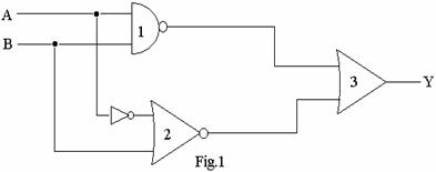
Q.3 a. Find the Boolean expression for logic circuit shown in Fig.1 below and reduce it using Boolean algebra. (6)
b. Reduce the following equation using K-map.
![]() (10)
(10)
Q.4 a. Explain the working of a tristate TTL gate. (8)
b. Explain various characteristics of digital ICs. (8)
Q.5 a. What is a multiplexer? Draw a gate level circuit and explain working of 4-to-1 multiplexer. (8)
b. Implement the following function using 4-to-1 multiplexer.
![]() (8)
(8)
Q.6 a. What is race around condition? How it can be avoided? (8)
b. With the help of a suitable diagram, explain the working of 4 bit serial in parallel out (SIPO) shift register. (8)
Q.7 a. Draw the circuit diagram of Asynchronous decade counter and explain its working. (8)
b. Design a mod-12 Synchronous up counter. (8)
Q.8 a. Explain the following for an ADC
(i) Input stage. (ii) Resolution.
(iii) Accuracy. (iv) Quantization error. (8)
b. Find how many bits of ADC are required to get an resolution of 0.5 mV if the maximum full scale voltage is 10 V. (8)
Q.9 a. What is a RAM? Explain the working of a Dynamic RAM cell. (8)
b. (i) How many ![]() RAM chips are
required to provide a memory capacity of 2048 bytes?
RAM chips are
required to provide a memory capacity of 2048 bytes?
(ii) How many lines of address bus must be used to access any one location of the 2048 bytes of memory designed in Q9 b (i)? How many lines of these will be common to each chip?
(iii) For the memory designed in Q9 b(i), how many bits are required to be decoded for chip-select signals. What is the size of the decoder used? (8)