Code:
DE-06 Subject:
BASIC ELECTRONICS 
Time: 3 Hours Max. Marks: 100
NOTE: There are 9 Questions in all.
· Question 1 is compulsory and carries 20 marks. Answer to Q. 1. must be written in the space provided for it in the answer book supplied and nowhere else.
· Out of the remaining EIGHT Questions answer any FIVE Questions. Each question carries 16 marks.
· Any required data not explicitly given, may be suitably assumed and stated.
Q.1 Choose the correct or best alternative in the following: (2x10)
a. Which of the following components are all active components
(A) A resistor and a capacitor.
(B) A microphone, a LCD and a Thyratron.
(C) An electric bulb, a transformer and a varactor diode.
(D) An SCR, a vacuum diode and an LED.
b. Doping materials are called impurities because they
(A) Decrease the number of charge carriers.
(B) Change the chemical properties of semiconductors.
(C) Make semiconductors less than 100 percent pure.
(D) Alter the crystal structures of the pure semiconductors.
c. Avalanche breakdown is primarily dependent on the phenomenon of
(A) Collision (B) Doping
(C) Ionisation (D) Recombination
d. In a rectifier, larger the value of shunt capacitor filter
(A) Larger the peak-to-peak value of ripple voltage.
(B) Larger the peak current in the rectifying diode.
(C) Longer the time that current pulse flows through the diode.
(D) Smaller the dc voltage across the load.
e. The main reason why electrons can tunnel through a P-N junction is that
(A) They have high energy.
(B) Barrier potential is very low.
(C) Depletion layer is extremely thin.
(D) Impurity level is low.
f. If a change in base current does not change the collector current, the transistor amplifier is said to be
(A) Saturated. (B) Cut-off.
(C) Critical. (D) Complemented.
g. The extremely high input impedance of a MOSFET is primarily due to the
(A) Absence of its channel.
(B) Negative gate-source voltage.
(C) Depletion of current carriers.
(D) Extremely small leakage current of its gate capacitor.
h. After firing an SCR, the gating pulse is removed. The current in the SCR will
(A) Remains the same. (B) Immediately fall to zero.
(C) Rise up. (D) Rise a little and then fall to zero.
i. An inverting
operational amplifier has ![]() and
and ![]() . Its scale factor is
. Its scale factor is
(A)
1000. (B)
![]() .
.
(C) ![]() . (D)
. (D)
![]() .
.
j. In the context of IC fabrication, metallisation means
(A) Connecting metallic wires.
(B) Forming interconnecting conduction pattern and bonding pads.
(C) Depositing ![]() layer.
layer.
(D) Covering with a metallic cap.
Answer any FIVE Questions out of EIGHT Questions.
Each question carries 16 marks.
Q.2 a. What do you mean by Passive components? Explain how the variable resistor can be used as a rheostat and Potentiometer with the help of symbols. Give their applications. (5)
b. What
is a Practical Current source; Explain its V-I characteristics. Convert an
a.c. current source of 2A in parallel with an impedance of ![]() into its equivalent
voltage source. (6)
into its equivalent
voltage source. (6)
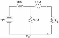
c. Determine
the current flowing through the load resistor ![]() when
when ![]() for the network shown below in Fig.1
by using Thevenin’s theorem. (5)
for the network shown below in Fig.1
by using Thevenin’s theorem. (5)
Q.3 a. Explain what do you understand by intrinsic, P-type and N-type semiconductors. Discuss the position of Fermi Level in each case with the help of Energy Band Diagram. (7)
b. Distinguish between Mobile Charge Carriers and Immobile Ions. (5)
c. Calculate the
Intrinsic conductivity of silicon at room temperature if ![]() ,
, ![]() ,
, ![]() and
and ![]() . What are the individual
contributions made by electrons and holes? (4)
. What are the individual
contributions made by electrons and holes? (4)
Q.4 a. What is breakdown diode? What is its use? Describe physically how two mechanisms of breakdown occurs in a p-n junction diode. (7)
b. Find the static and the
dynamic resistance of a p-n junction Germanium diode, if the temperature is ![]() and
and ![]() for an applied
forward bias of 0.2V. (4)
for an applied
forward bias of 0.2V. (4)
c. What is Schottky diode? Why is it also called Hot-Carrier diode? How does it differ in construction from a normal P-N junction diode. (5)
Q.5 a. Draw the circuit diagram of Four-diode Full-wave Bridge Rectifier and explain its operation. What are its advantages and disadvantages. (6)
b. A
half-wave rectifier using silicon diode has a secondary e.m.f of 14.14V
(r.m.s.) with a resistance of ![]() . The diode has a forward resistance
of 0.05
. The diode has a forward resistance
of 0.05![]() and a threshold voltage of 0.7V. If the load resistance is 10
and a threshold voltage of 0.7V. If the load resistance is 10![]() . Determine
. Determine
(i) d.c. load current. (ii) d.c. load voltage.
(iii) Voltage regulation. (iv) Efficiency. (5)
c. Draw the functional block diagram of Three-Terminal Voltage Regulator IC and describe its operation. (5)
Q.6 a. Define a Transistor. Draw the circuit diagrams of p-n-p and n-p-n transistors with proper biasing voltages. Also indicate the reference directions for the currents and the reference polarities for the voltage. (5)
b. Define Transistor characteristics? Sketch the output characteristics of a transistor in its CB mode. Explain the Active, cut-off and saturation Regions. (7)
c. The current gain ![]() of an n-p-n transistor is 0.98. It
is connected in the CB mode and gives a reverse saturation current
of an n-p-n transistor is 0.98. It
is connected in the CB mode and gives a reverse saturation current ![]() . Find the Base
and the collector currents for an Emitter current of 2mA. (4)
. Find the Base
and the collector currents for an Emitter current of 2mA. (4)
Q.7 a. What is MOSFET? How does MOSFET differ from JFET? Why MOSFETs are more widely used than the JFETs? (4)
b. Draw the structure of an N-channel JFET and explain its principle of operation with neat diagrams along with V-I characteristics. Define Pinch-off voltage and mark it on the characteristics. Explain its significance in the operation of JFET. (8)
c. Determine
the Pinch-off voltage for an N-channel silicon JFET with a channel width of ![]() and a donor
concentration of
and a donor
concentration of ![]() ; Given that dielectric constant of
silicon is 12. (4)
; Given that dielectric constant of
silicon is 12. (4)
Q.8 a. What is an SCR? Explain the construction, working and V-I characteristics of an SCR for different gate currents and indicate there-upon holding current, latching current and breakover voltage. (8)
b. What is an integrated circuit? Explain how a capacitor can be constructed in a monolithic IC. (4)
c. What is photo-electric emission? Explain how is this emission affected if the frequency and the intensity of the incident radiations are increased. (4)
Q.9 a. Draw the circuit of an OP-AMP Differential Amplifier and derive an expression for its output voltage. (5)
b. In the circuit shown below in Fig.2, calculate
(i) ![]() (ii)
(ii) ![]() (iii)
The Load Current
(iii)
The Load Current ![]()
(iv)
The output current ![]() indicating proper direction of flow. (6)
indicating proper direction of flow. (6)

c. Explain the operation of an OPAMP current-to-voltage converter with the help of circuit diagram. (5)