Code:
DC-02 Subject: FUNDAMENTALS OF
ELECTRONICS 
Time: 3 Hours Max. Marks: 100
NOTE: There are 9 Questions in all.
· Question 1 is compulsory and carries 20 marks. Answer to Q. 1. must be written in the space provided for it in the answer book supplied and nowhere else.
· Out of the remaining EIGHT Questions answer any FIVE Questions. Each question carries 16 marks.
· Any required data not explicitly given, may be suitably assumed and stated.
Q.1 Choose the correct or best alternative in the following: (2x10)
a. If the sequence of colour bands on a resistor is yellow, violet, orange, and gold then, the value of the resistance is
(A)
![]() with
with ![]() 5% tolerance. (B)
5% tolerance. (B)
![]() with
with
![]() 5%
tolerance.
5%
tolerance.
(C)
![]() with
with ![]() 5% tolerance. (D)
5% tolerance. (D)
![]() with
with
![]() 5%
tolerance.
5%
tolerance.
b. A constant current source supplies a current of 300 mA to a load of
1![]() . When
the load is changed to 100
. When
the load is changed to 100![]() , the load current will be
, the load current will be
(A) 3A (B) 30 mA
(C) 300 mA (D) 600 mA
c. The forbidden energy gap in semiconductors
(A) lies just below the valence band.
(B) lies just above the conduction band.
(C) lies between the valence band and the conduction band.
(D) is the same as the valence band.
d. In the forward bias condition of a semiconductor diode for a change in voltage from 0.73 to 0.66 V the corresponding change in current is from 17.5 to 10 mA. The dynamic resistance of the diode is then equal to
(A)
8.46 ![]() (B)
10.46
(B)
10.46 ![]()
(C) 9.46 ![]() (D)
7.46
(D)
7.46 ![]()
e. The depletion region in the PN-Junction formed in the tunnel diode fabrication will be of the order of
(A)
![]() (B)
(B)
![]()
(C) ![]() (D)
(D)
![]()
f. If the feedback factor in a negative feedback amplifier is –0.5, and the gain of the basic amplifier without feedback is –100, then the overall voltage gain with feedback is
(A) –2.96 (B) –3.96
(C) –1.96 (D) –5
g. The complement of
the function ![]() is
is
(A)
![]() (B)
(B)
![]()
(C) ![]() (D)
(D) ![]()
h. The accepted temperature ranges in which an IC functions properly, for military applications is
(A)
0 to ![]() (B)
(B)
![]() to
to ![]()
(C) – 55 to ![]() (D) 10
to
(D) 10
to ![]()
i. For the OPAMP
circuit shown in Fig.1, the value of ![]() is
is
|
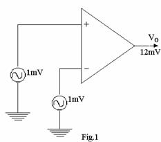
(A) 9 (B) 15
(C) 22 (D) 12
j. In IC technology for most semiconductor fabrications, the impurity levels of less than
(A) One part in two billions are required.
(B) One part in 4 billions are required.
(C) One part in one billion are required.
(D) Two parts in 4 billions are required.
Answer any FIVE Questions out of EIGHT Questions.
Each question carries 16 marks.
Q.2 a. What is an inductor? What is its measuring unit? Write the circuit symbols for an air-core and iron-core inductor. Write three lines about audio-frequency chokes. (7)
b. Write the name of three active components of the solid state type other than the conventional PN junction diode and the BJT. (3)
c. What do you mean by thermionic emission in a vacuum tube? Name four active electronic components of the vacuum tube type. (6)
Q.3 a. Distinguish between intrinsic and extrinsic semi-conductors. What is the effect of temperature on extrinsic semiconductors? (7)
b. What is a semiconductor diode? When do you say that a given diode is ideal? How does the V-I characteristics of such a diode look like? Briefly explain. Suggest an application for the ideal diode. (9)
Q.4 a. What is an LED? What is the material used in an LED that emit invisible radiation? Write one application for such an LED. What are the advantages of LEDs? (9)
b. What are the advantages and disadvantages of LCDs? (3)
c. What is the special feature of a tunnel diode as compared to other diodes? How is a tunnel diode fabricated? (4)
Q.5 a. What is a transistor? Define the following for a transistor:
(i) ![]() (ii)
(ii)
![]()
What is ac alpha formally called? Explain the basic amplifying action of the transistor at the surface level using a common-base configuration as an example. (12)
b. Briefly explain the basic construction of the n-channel JFET, with a sketch for illustration. (4)
Q.6 a. What is the effect of positive feedback on a basic amplifier circuit? What are the improvements of the basic amplifier obtained with negative feedback? (5)
b. What do you mean by the following:
i. Voltage-shunt feedback.
ii. Current-series feedback. (8)
Write the schematics for the above. (6)
c. Write
the circuit of a Colpitts oscillator using FET. What is the expression for its
frequency of oscillations? If in the above circuit, the values of L, C1
and C2 are: ![]() ,
, ![]() and
and ![]() respectively, calculate the
frequency of oscillations. (5)
respectively, calculate the
frequency of oscillations. (5)
Q.7 a. Define the following operations of the digital system and illustrate their standard symbols:
(i) The NAND operation
(ii) The NOR operation
Write the truth tables for the above operations, assuming two-input logic gates. Also illustrate how the OR, and AND operations can be realised using only NAND logic. (8)
b. A four variable logic function is given below.
![]()
Obtain the K-map for the function given and write the minimised Boolean expression. (8)
Q.8 a. Which are the commonly used bipolar logic families of the non-saturated type? What are the main elements of a unipolar logic family? List the logic families of this category. (6)
b. What do you mean by the following terms of digital ICs:
(i) Speed of operation.
(ii) Power dissipation. (5)
c. Write the circuit of a 3-input DTL NAND gate and briefly explain. (5)
Q.9 a. What is an OPAMP? Which is the important feature of a differential circuit connection, provided in an OPAMP? Write the defining equations for the following quantities as applied to an OPAMP:
(i) Differential Inputs.
(ii) Common inputs.
(iii) Output voltage. (9)
b. Determine
the output voltage of an OPAMP for input voltages of 150 ![]() & 140
& 140 ![]() at its input terminals. Take
at its input terminals. Take ![]() as 4000 and CMRR
as 100. (4)
as 4000 and CMRR
as 100. (4)
c. Briefly explain a 3-input summing amplifier of the inverting type using an OPAMP. (3)