Code:
AE-05 Subject:
BASIC ELECTRONICS 
Time: 3 Hours Max. Marks: 100
NOTE: There are 9 Questions in all.
· Question 1 is compulsory and carries 20 marks. Answer to Q. 1. must be written in the space provided for it in the answer book supplied and nowhere else.
· Out of the remaining EIGHT Questions answer any FIVE Questions. Each question carries 16 marks.
· Any required data not explicitly given, may be suitably assumed and stated.
Q.1 Choose the correct or best alternative in the following: (2x10)
a. The breakdown mechanism in a lightly doped p-n junction under reverse biased condition is called
(A) avalanche breakdown.
(B) zener breakdown.
(C) breakdown by tunnelling.
(D) high voltage breakdown.
b. In a CE connected transistor amplifier with voltage gain ![]() , the capacitance
, the capacitance ![]() is amplified by a
factor
is amplified by a
factor
(A)
![]() (B)
(B)
![]()
(C)![]() (D)
(D)
![]()
because of Miller effect.
c. For large values
of ![]() , a
FET behaves as
, a
FET behaves as
(A) Voltage controlled resistor.
(B) Current controlled current source.
(C) Voltage controlled current source.
(D) Current controlled resistor.
d. Removing bypass capacitor across the emitter leg resistor in a CE amplifier causes
(A) increase in current gain. (B) decrease in current gain.
(C) increase in voltage gain. (D)decrease in voltage gain.
e. For an op-amp
having differential gain ![]() and common mode gain
and common mode gain ![]() the CMRR is given
by
the CMRR is given
by
(A)
![]() (B)
(B)
![]()
(C) ![]() (D)
(D) ![]()
f. When a step input is given to an op-amp integrator, the output will be
(A) a ramp.
(B) a sinu-soidal wave.
(C) a rectangular wave.
(D) a triangular wave with dc bias.
g. Hystersis is desirable in Schmitt trigger, becuase
(A) energy is to be stored/discharged in parasitic capacitances.
(B) effects of temperature would be compensated.
(C) devices in the circuit should be allowed time for saturation and desaturation.
(D) it would prevent noise from causing false triggering.
h. In a full-wave rectifier without filter, the ripple factor is
(A) 0.482 (B) 1.21
(C) 1.79 (D) 2.05
i. A minterm of the Boolean function, f(x, y, z) is
(A) ![]() (B)
(B) ![]()
(C) x z (D) (y +z) x
j. The minimum number of flip-flops required to construct a mod-75 counter is
(A) 5 (B) 6
(C) 7 (D) 8
Answer any FIVE Questions out of EIGHT Questions.
Each question carries 16 marks.
Q.2 a. A triangular wave shown in figure (1) is applied to the circuit in figure (2). Explain the working of the circuit. Sketch the output waveform. (7)
 |
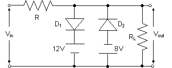 |
Figure (1) Figure (2)
b. Define ‘diffusion capacitance’ of a pn junction diode. Obtain an expression for the same. Why is the diffusion capacitance negligible for a reverse biased diode? (9)
Q.3 a. Draw the circuit of h-parameter equivalent of a CE amplifier with unby-passed emitter resistor. Derive an expression for (i) its input impedance and (ii) voltage gain, using the equivalent circuit. (10)
b. What is a ‘multistage amplifier’? Give the requirements to be fulfilled for an ideal coupling network. (6)
Q.4 a. Draw a neat sketch to illustrate the structure of a N-channel E-MOSFET. Explain its operation. (9)
b. A class B push-pull
amplifier is supplied with ![]() . The minimum voltage reached by the
collector due to signal swing is
. The minimum voltage reached by the
collector due to signal swing is ![]() . The dissipation in both the
transistors totals 30 W. What is the conversion efficiency of the amplifier? (7)
. The dissipation in both the
transistors totals 30 W. What is the conversion efficiency of the amplifier? (7)
Q.5 a. Show that in an amplifier, the gain reduces if negative feedback is used. (6)
b. In a voltage series feedback amplifier, show that
(i) the input impedance increases with negative feedback.
(ii) the output impedance decreases due to negative feedback. (10)
Q.6 a. List the advantages of a crystal oscillator. (4)
b. The input to an op-amp
differentiator circuit is a sinusoidal voltage of peak value ![]() and frequency of
2 kHz. If the values of differentiating components are given as R = 40 k
and frequency of
2 kHz. If the values of differentiating components are given as R = 40 k![]() and C =
and C = ![]() , determine the
output voltage. (4)
, determine the
output voltage. (4)
c. Draw the block diagram representation of a typical op-amp. Explain the function of each block briefly. (8)
Q.7 a. Draw
the circuit of a monostable multivibrator using two transistors. Use the
following data in your circuit: ![]() ,
, ![]() , B
, B![]() ,
, ![]() for both the transistors. The
resistor and capacitor connected to the base of
for both the transistors. The
resistor and capacitor connected to the base of ![]() have values
have values ![]() and C = 0.1
and C = 0.1 ![]() respectively.
Determine the monostable pulse width. (8)
respectively.
Determine the monostable pulse width. (8)
b. Explain how the timer IC 555 can be operated as an astable multivibrator, using timing diagrams. (8)
Q.8 a. Draw the circuit of a bridge rectifier using capacitor filter and explain its working by drawing input and output waveforms. (8)
b. For
the series regulator given below, ![]() ,
, ![]() , the transistor
, the transistor ![]() ,
, ![]() =1.2 K
=1.2 K![]() ,
, ![]() =10V and
=10V and ![]() . Calculate (i)
output voltage (ii) load current (iii) the base current in the transistor (iv)
zener current. (8)
. Calculate (i)
output voltage (ii) load current (iii) the base current in the transistor (iv)
zener current. (8)
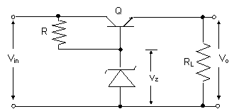 |
Q.9 a. Draw the truth table of a Full Adder circuit. Obtain the simplified expressions for the ‘sum’ and ‘carry’ outputs of the adder and draw its logic diagram using suitable gates. (9)
b. What is a synchronous counter? Draw the circuit of a three-bit synchronous up-down counter and explain its operation. (7)