Code: AC-03 / AT-03 Subject: BASIC
ELECTRONICS & DIGITAL CIRCUITS 
Time: 3 Hours Max. Marks: 100
NOTE: There are 9 Questions in all.
· Question 1 is compulsory and carries 20 marks. Answer to Q. 1. must be written in the space provided for it in the answer book supplied and nowhere else.
· Out of the remaining EIGHT Questions answer any FIVE Questions. Each question carries 16 marks.
· Any required data not explicitly given, may be suitably assumed and stated.
Q.1 Choose the correct or best alternative in the following: (2x10)
a. If the resistivity of a sample of N-type semiconductor with a Hall coefficient of 160 cm3/coulumb is 0.16 ohm-cm, then the mobility of the electron in the sample is
(A) 950 cm2/volt-sec (B) 1000 cm2/volt-sec
(C) 570 cm2/volt-sec (D) 462 cm2/volt-sec
b. Allow 0.7 V for the VBE drop in the circuit given. The dc collector-base voltage will be
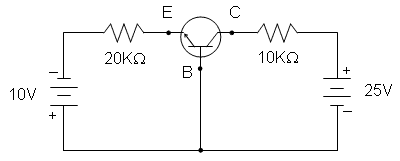
(A) 16 V
(B) 10 V
(C) 20 V
(D) 25 V
c. The h-parameters are called hybrid parameters because they
(A) are different from impedance and admittance parameters
(B) apply to circuits contained in a box
(C) are defined by using both short circuit and open circuit terminations
(D) are mixed with other parameters
d. The voltage gain of a Darlington amplifier is
(A) equal to unity
(B) less than unity
(C) greater than unity
(D) equal to zero
e. The N-channel MOSFET devices are preferred more than P-channel ones because
(A) N-channel devices are faster than P-channel devices
(B) N-channel devices have higher packing density than P-channel devices
(C) N-channel devices consume less power than P-channel devices
(D) Both (A) and (B) above,
f. If the parameters of a crystal are: L=0.33H, C1=0.065 pF, C2=1pF and R=5.5KW, with usual notations, then the series resonant frequency is
(A) 2.12 MHz (B) 1.09 MHz
(C) 1.8 MHz (D) 2.5 MHz
g. A three-variable Boolean expression in m-notation is f(xyz) = Sm(0,4,7). Its algebraic form is
(A)
![]() (B)
(B)
![]()
(C) ![]() (D)
(D) ![]()
h. When (1010)2 is subtracted from (1111)2 using 2’s complement method, the result is
(A) (0101)2 (B) (1011)2
(C) (1101)2 (D) (0011)2
i. The propagation delay time of a typical ECL gate is
(A) 5 ns (B) 8 ns
(C) 1 ns (D) 6.2 ns
j. In a ROM how many words are addressed using 18 address bits?
(A) 200 K (B) 2 K
(C) 256 K (D) 138 K
Answer any FIVE Questions out of EIGHT Questions.
Each question carries 16 marks.
Q.2 a. Define a semiconductor in terms of energy bands and comment in brief on free charge carriers in semiconductors. (8)
b. A 4.7 V zener diode has a resistance of 15W. What is the terminal voltage when the current is 20 mA? (3)
c. A sinosoidal signal of peak voltage Vm is applied to a diode circuit to generate the waveform shown. Draw the diode circuit and briefly explain its operation.
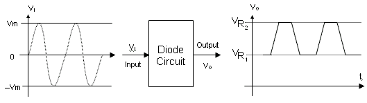
Assume that the Peak of the
input voltage is greater than ![]() . (5)
. (5)
Q.3 a. Draw the hybrid model for a transistor and write the equations for the input voltage and output current for the above model. Define the hybrid parameters involved. (7)
b. For the amplifier circuit shown below, calculate Ri, Ai, Av.

The h-parameters for the transistor are: hic=1.2KW, hfc=101, hrc=1, hoc=25A/V. (9)
Q.4 a. FET amplifiers have become more popular than BJT amplifiers. Give reasons. Draw the circuit of a common-source amplifier using N-channel enhancement FET and draw its a.c. equivalent circuit. Deduce the equation for its voltage gain. (13)
b. Write the basic configuration for any resonant circuit oscillator that uses an OP AMP and give its linear equivalent circuit. (3)
Q.5 a. Illustrate neatly the basic operational amplifier in terms of its circuit symbol and draw its low-frequency equivalent circuit. What do you mean by single-ended amplifier? (5)
b. With neat sketches for illustration, explain the operation of the circuit shown below, by taking the voltage Vin as a sinosoidal signal and VRef equal to zero. (6)

|
c. (i) Assuming the diode in the circuit shown to be an ideal one, calculate the dc output for the network shown below for the input voltage indicated.
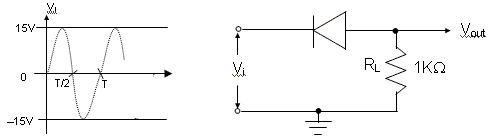
(ii) Repeat the above calculation by replacing the diode with a silicon diode of cut-in voltage 0.7 V. Take the forward resistance of the diode as zero. (5)
Q.6 a. Prove the following property of Boolean algebra
A + BC = (A + B) (A + C) (4)
b. Simplify the Boolean function given using Karnaugh Map method
¦![]() (7)
(7)
c. Write the truth table and logic diagram of a one-to-four demultiplexer using inverters and AND gates only. (5)
Q.7 a. Write a note on FET switches. (7)
b. When do you use NMOS logic circuits? Write a brief note on CMOS logic. Write the circuit of a two-input CMOS NAND gate. (9)
Q.8 a. Briefly explain the following TTL parameters:
(i) Fan-out (ii) Noise immunity (5)
b. What is a RAM? Write the block schematic of a RAM and briefly explain. (11)
Q.9 a. What is a Flip-Flop? Which are the different types commonly used? Explain how an S-R Flip-Flop can be constructed using two NOR gates and comment on its truth table. (8)
b. What is the primary function of a counter? Write the schematic of a four-bit binary UP-counter using positive edge triggered T flip-flops, and briefly explain. (8)