DipIETE – ET (NEW SCHEME) – Code: DE56
Subject: ANALOG ELECTRONICS
 Time: 3
Hours
Max. Marks: 100
Time: 3
Hours
Max. Marks: 100
NOTE: There are 9 Questions in all.
· Question 1 is compulsory and carries 20 marks. Answer to Q. 1. must be written in the space provided for it in the answer book supplied and nowhere else.
· Out of the remaining EIGHT Questions answer any FIVE Questions. Each question carries 16 marks.
· Any required data not explicitly given, may be suitably assumed and stated.
Q.1 Choose
the correct or the best alternative in the following: (2![]() 10)
10)
a. Small scale integration (SSI) chip contains approximately
(A) 10 transistors (B) 100 transistors
(C) 1000 transistors (D) 10000 transistors
b. The purpose of using emitter bypass capacitor in a voltage amplifier is to
(A) avoid ac degeneration (B) increase input impedance
(C) decrease input impedance (D) decrease output impedance
c. The voltage gain of common collector amplifier is
(A) < 1 (B) > 1
(C) > 10 (D) < 10
d. FET is a
(A) current operated device (B) power operated device
(C) resistance operated device (D) voltage operated device
e. The maximum power conversion efficiency of Class A transformer coupled power amplifier is
(A) 25% (B) 75%
(C) 50% (D) 78.5%
f. The material used in light emitting diode is
(A) Silicon (B) Germanium
(C) Glass (D) Gallium arsenide
g.
The slew rate of an opamp with an internal capacitor of 30 pF and maximum
internal capacitor charging current of 15![]() is
is
(A) ![]() (B)
(B)
![]()
(C) ![]() (D)
(D)
![]()
h. Commonly used audio power amplifier chip is
(A)
![]() (B)
LM 380
(B)
LM 380
(C) 7400 (D) 555
i. The input to Astable multivibrator is
(A) sine wave (B) square wave
(C) triangular wave (D) no input
j. The fastest type of ADC is
(A) counter type (B) flash type
(C) dual-slope type (D) successive approximation type
Answer any FIVE Questions out of EIGHT Questions.
Each question carries 16 marks.
Q.2 a. List the basic processes used in the silicon planar technology and describe photolithography and diffusion processes. (12)
b. Write an explanatory note on thin and thick film technology. (4)
Q.3 a. Derive expressions for input impedance, output impedance, voltage gain and current gain of CE transistor amplifier with voltage divider bias using h model with emitter resistor by passed. (10)
b. Calculate ![]() and
and ![]() for a common collector circuit with
the following component values and parameters.
for a common collector circuit with
the following component values and parameters. ![]()
![]()
![]()
![]()
![]()
![]()
![]() . (6)
. (6)
Q.4 a. With neat diagram explain the working of enhancement mode MOSFET. (10)
b. A
JFET is used in the amplifier circuit shown in Fig.1. Calculate the minimum
and maximum voltages produced by a
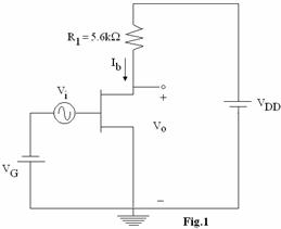
![]() AC input. Also calculate the
circuit voltage gain in each case. Assume
AC input. Also calculate the
circuit voltage gain in each case. Assume ![]() and
and ![]() . (6)
. (6)
Q.5 a. With a neat diagram explain the working of a transformer coupled Class-B power amplifier and obtain an expression for theoretical maximum power efficiency. (10)
b. Explain the working of a photo-transistor with appropriate sketches. (6)
Q.6 a. Draw the circuit of practical Opamp inverting amplifier and explain. Derive expressions for:
(i) closed loop voltage gain.
(ii) input resistance
(iii) output resistance. (10)
b. For
the non-inverting amplifier shown in Fig.2, ![]()
![]() .
.
(i)
Calculate the maximum output offset voltage due to ![]() and
and ![]()
![]() .
.
(ii)
Calculate the value of ![]() to reduce the effect of
to reduce the effect of ![]() .
.
(iii)
Calculate the maximum output offset voltage if
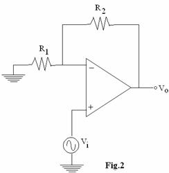
![]() as calculated in the above part (ii)
is connected to the circuit. (6)
as calculated in the above part (ii)
is connected to the circuit. (6)
Q.7 a. Draw the circuit of an instrumentation amplifier using three Opamps. Derive expression for output voltage. (8)
b. Find
the values of ![]() and
and
![]() in the
lossy integration circuit using Opamp so that the peak gain is 20 dB. At
in the
lossy integration circuit using Opamp so that the peak gain is 20 dB. At ![]() the gain decreases by 3 dB from
its peak. Use a capacitance of
the gain decreases by 3 dB from
its peak. Use a capacitance of ![]() . (8)
. (8)
Q.8 a. Draw the circuit of a square wave generator using 555 timer. Draw the various waveforms and derive an expression for time period T. (10)
b. Design
an inverting schmitt trigger circuit having ![]() and
and ![]() . Assume saturated output voltage as
. Assume saturated output voltage as
![]() . Draw
the transfer characteristics. (6)
. Draw
the transfer characteristics. (6)
Q.9 a. With a diagram and waveforms explain the working of a dual slope ADC. (10)
b. Using
7805 voltage regulator, design a current source to deliver 0.2 A current to a ![]() , 10 W load. Draw
the diagram with component values. (6)
, 10 W load. Draw
the diagram with component values. (6)