DipIETE – ET (OLD SCHEME)
 Code:
DE09 Subject:
DIGITAL ELECTRONICS
Code:
DE09 Subject:
DIGITAL ELECTRONICS
Time: 3 Hours Max. Marks: 100
NOTE: There are 9 Questions in all.
· Question 1 is compulsory and carries 20 marks. Answer to Q. 1. must be written in the space provided for it in the answer book supplied and nowhere else.
· Out of the remaining EIGHT Questions answer any FIVE Questions. Each question carries 16 marks.
· Any required data not explicitly given, may be suitably assumed and stated.
Q.1 Choose
the correct or the best alternative in the following: (2![]() 10)
10)
a. The 2’s complement of the number 1101101 is
(A) 0010010. (B) 0010011.
(C) 0110011. (D) 0011111.
b. The digital logic family which has the lowest power dissipation per gate is
(A) DTL. (B) CMOS.
(C) MOS. (D) TTL.
c. In a negative logic system, logic state 1 is represented by
(A) positive voltage. (B) zero voltage.
(C) negative voltage. (D) none.
d. The commercially available 16 input multiplexer integrated circuit in TTL family is
(A) 74150. (B) 74151.
(C) 74157. (D) 74153.
e. The number of control lines required for 32:1 multiplexer is
(A) 2. (B) 4.
(C) 3. (D) 5.
f. How many two input AND and two input OR gates are required to realize Y=ABC+DE+F?
(A) 3,2. (B) 2,1.
(C) 2,2. (D) 2,3.
g. A 4-bit asynchronous counter uses flipflops with propagation delay times of 20 ns each. The maximum possible time required for change of state will be
(A) 20 ns. (B) 40 ns.
(C) 0 ns. (D) 80 ns.
h. Which of the following memory is non volatile?
(A) DRAM. (B) SRAM.
(C) ROM. (D) none.
i. When simplified
with Boolean Algebra ![]() reduces to?
reduces to?
(A)
AB. (B)
![]() .
.
(C) ![]() . (D)
. (D)
![]() .
.
j. When the set of input data to an even parity generator is 0110101, the output will be?
(A) 1. (B) 0.
(C) can not say. (D) none.
Answer any FIVE Questions out of EIGHT Questions.
Each question carries 16 marks.
Q.2 a. Convert
![]() to
hexadecimal number system. (8)
to
hexadecimal number system. (8)
b. Express – 45 in 8 bit 2’s complement form. (8)
Q.3 a. Show
that ![]() . (8)
. (8)
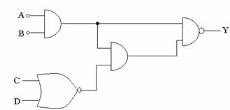
b. Use the Demorgan’s theorem and Boolean algebraic expressions to simplify the circuit shown below. (8)
Q.4 a. Explain the operations of CMOS invertor and state advantages of CMOS. (8)
b. Draw K-map for the following function and reduce it
![]() (8)
(8)
Q.5 a. What is full subtractor? Design the logic circuit for it. (10)
b. Use the multiplexer to implement the function
![]() (6)
(6)
Q.6 a. Design a 4 line to 16 line decoder using 2 line to 4 line decoder. (8)
b. What is race around condition? How can it be avoided? (8)
Q.7 a. Design a mod-12 asynchronous counter. (8)
b. Explain the working and operation of PISO. (8)
Q.8 a. Explain the performance characteristics of D/A converter. (8)
b. Explain the operation of Dual slope A/D converter. (8)
Q.9 a. The
capacity of ![]() PROM
is to be expanded to
PROM
is to be expanded to ![]() . How many PROM chips are required?
Show the arrangement. (8)
. How many PROM chips are required?
Show the arrangement. (8)
b. What is DRAM refreshing? Explain how it is done. (8)