DipIETE – ET (OLD SCHEME)
 Code:
DE08
Subject: ANALOG ELECTRONICS
Code:
DE08
Subject: ANALOG ELECTRONICS
Time: 3 Hours Max. Marks: 100
NOTE: There are 9 Questions in all.
· Question 1 is compulsory and carries 20 marks. Answer to Q. 1. must be written in the space provided for it in the answer book supplied and nowhere else.
· Out of the remaining EIGHT Questions answer any FIVE Questions. Each question carries 16 marks.
· Any required data not explicitly given, may be suitably assumed and stated.
Q.1 Choose
the correct or the best alternative in the following: (2![]() 10)
10)
a. The biasing circuit which gives the best stability to the Q point is
(A) Base resistor biasing (B) Feedback resistor biasing
(C) Potential divider biasing (D) Emitter resistor biasing
b. If
![]() and
and ![]() are collector and load
resistors respectively then AC load resistance will be
are collector and load
resistors respectively then AC load resistance will be
(A)
![]() (B)
(B)
![]()
(C) ![]() (D)
(D)
![]()
c. A push pull amplifier
(A) reduces odd harmonics in O/P.
(B) is the first stage of audio amplifier.
(C) reduces even harmonics in O/P.
(D) uses single transistor.
d. The negative feedback in an amplifier
(A) increases the voltage gain. (B) decreases the voltage gain.
(C) stabilizes the voltage gain. (D) both (B) and (C).
e. The Barkhausen criterion for oscillation is stated as
(A)
![]() . (B)
. (B)
![]() .
.
(C) ![]() . (D)
. (D)
![]() .
.
f. In a double tuned amplifier circuit
(A) two transistors are employed.
(B) two tuning circuits are used.
(C) two input signals are fed.
(D) none of the above.
g. A FET is characterized by
(A) Current gain. (B) Voltage gain.
(C) Power gain. (D) None of the above.
h. The gain of an op-amp voltage follower is
(A) Zero. (B) unity.
(C) infinity. (D) very high.
i. If a square wave is fed to a differentiating circuit, the output will be
(A) Sharp narrow pulses. (B) Triangular wave.
(C) Sawtooth wave. (D) Sine wave.
j. A high Q tuned circuit in an amplifier permits to have
(A) selectivity. (B) fidelity.
(C) sensitivity. (D) frequency range.
Answer any FIVE Questions out of EIGHT Questions.
Each question carries 16 marks.
Q.2 a. Draw and explain the circuit diagram of fixed biasing. (8)
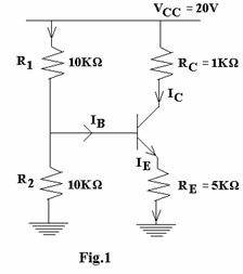
b. Calculate the emitter current in the voltage divider circuit shown in Fig.1. Also find the value of the VCE and collector potential VC . (8)
Q.3 a. Derive an expression for maximum collector efficiency of series fed Class-A amplifier. (8)
b. (i) A power transistor has thermal resistance Q=300C/W. If maximum junction temperature is 90°C and the ambient temperature is 30°C. Find the maximum permissible power dissipation.
(ii) If a heat sink is used with the above transistor, the value of Q is reduced to 60°C/W. Find the maximum permissible power dissipation. (8)
Q.4 a. State the advantages of negative feedback. (8)
b. Explain the operation of transistor as a switch. (8)
Q.5 a. Draw the hybrid pi model for transistor in CB configuration and briefly explain the components of the model. (8)
b. A
Class-A power amplifier has a transformer as the load. If the transformer has a
turn ratio of 10 and a secondary load is![]() , find the maximum AC power output.
Given that zero signal collector current is 100 mA. (8)
, find the maximum AC power output.
Given that zero signal collector current is 100 mA. (8)
Q.6 a. Draw the circuit diagram of Hartley oscillator and explain its working. (8)
b. In phase shift
oscillator ![]() and
and
![]() At
what frequency does the circuit oscillate? (8)
At
what frequency does the circuit oscillate? (8)
Q.7 a. Draw and explain the operation of a comparator using op-amp. (8)
b. Draw and explain the circuit diagram of relaxation oscillator using UJT. (8)
Q.8 a. Draw the inverting amplifier using op-amp and derive the equation for voltage gain. (8)
b. The
voltage of ![]() and
and
![]() are
applied to the two input resistors of a summing amplifier. The respective input
resistors are
are
applied to the two input resistors of a summing amplifier. The respective input
resistors are ![]() and
and
![]() and
feedback resistor is
and
feedback resistor is ![]() . Find the output voltage. (8)
. Find the output voltage. (8)
Q.9 a. Draw the circuit diagram of double tuned amplifier and explain its working. . (8)
b. Describe the operation of 555 timer as an astable multivibrator. (8)