AMIETE – ET/CS/IT (NEW SCHEME) – Code: AE54/AC54/AT54
Subject: LINEAR ICs & DIGITAL ELECTRONICS
 Time: 3
Hours
Max. Marks: 100
Time: 3
Hours
Max. Marks: 100
NOTE: There are 9 Questions in all.
· Question 1 is compulsory and carries 20 marks. Answer to Q. 1. must be written in the space provided for it in the answer book supplied and nowhere else.
· Out of the remaining EIGHT Questions answer any FIVE Questions. Each question carries 16 marks.
· Any required data not explicitly given, may be suitably assumed and stated.
Q.1 Choose
the correct or the best alternative in the following: (2![]() 10)
10)
a. The number of transistors per chip in a VERY LARGE SCALE INTEGRATED CIRCUIT is
(A) 100 – 1,000 (B) 1000 – 20,000
(C) 20,000
– 10,00,000 (D) ![]()
b.
The number of IC chips of size 2 mm ![]() 2 mm that could be fabricated on an 8”
diameter silicon wafer is
2 mm that could be fabricated on an 8”
diameter silicon wafer is
(A) 31,400 (B) 15,700
(C) 7850 (D) 3925
c. If an Op Amp has 5 terminals (2 input, 1 output and 2 supply voltage terminals), the number of pins required for a single package to house 4 such Op amps are
(A) 20 (B) 14
(C) 16 (D) 12
d. If an Op Amp is specified to have its common mode and differential mode gains as 25 and 100,000 respectively, then its Common Mode Rejection Ratio (CMRR) is
(A) 60 dB (B) 66 dB
(C) 72 dB (D) 100 dB
e. If
the slew rate of an Op amp is ![]() and when the Op amp is used as a
voltage follower, the maximum amplitude of the sinusoidal input signal of 100
KHz frequency that could be applied, so that the output is undistorted is
and when the Op amp is used as a
voltage follower, the maximum amplitude of the sinusoidal input signal of 100
KHz frequency that could be applied, so that the output is undistorted is
(A) 3.14 V (B) 2 V
(C) 6.28 V (D) 12.56 V
f. A triangular wave form could be generated by _________ a square waveform.
(A) Differentiating (B) Integrating
(C) Squaring (D) Inverting
g. The combination of Arithmetic/Logic unit and the control unit is called _________.
(A) Microprocessor (B) Control Processing Unit
(C) Microcontroller (D) Full Adder
h. In the BCD code each _________ is converted into its 4 bit binary equivalent.
(A) Decimal (B) Digit
(C) Byte (D) Nibble
i. Input impedance and output impedance of an ideal op-amp should be
(A) ![]() (B)
(B)
![]()
(C) ![]() (D)
(D)
![]()
j. A ripple counter using 4 JK Flip Flops has a count 0101 initially. What will be its count after 27 clock pulses?
(A) 0101 (B) 1111
(C) 1010 (D) 0000
Answer any FIVE Questions out of EIGHT Questions.
Each question carries 16 marks.
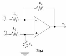
Q.2 a. Prove that in the
differential amplifier circuit of Fig.1, the output voltage ![]() only if
only if ![]() . (8)
. (8)
b. Calculate
the differential gain ![]() and common mode gain
and common mode gain ![]() of the above
circuit, if
of the above
circuit, if ![]() and
and
![]() and
and ![]() . (8)
. (8)
Q.3 a. Draw the circuit of an instrumentation amplifier using 3 ideal Op amps, and choose appropriate values for the different resistors so that the output is proportional to the differential input. For the chosen values of resistors, determine the gain of the amplifier. (8)
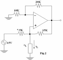
b. In the voltage to current
converter circuit of Fig.2, determine the current
![]() through
through ![]() . Assume an ideal Op amp. (8)
. Assume an ideal Op amp. (8)
Q.4 a. Show how an ideal Op amp could be used as a differentiation. Draw the circuit of a practical differentiation and explain how this circuit eliminates the problems in a simple differentiator circuit. (8)
b. Design
an inverting Schmitt trigger circuit to have its ![]() . Assume
. Assume ![]() . (8)
. (8)
Q.5 a. Describe the functioning of a Successive Approximation Analog to Digital (A/D) converter using a suitable block diagram. (8)
b. Design an Astable multivibrator circuit using 555 timer IC, to obtain an output frequency of 5 KHz with a duty ratio of 30 %. (8)
Q.6 a. Prepare a table showing the binary, octal, hexadecimal and BCD representations of all decimal nos from 23 to 33. (8)
b. Convert the following as indicated
(i)
![]() (ii)
(ii)
![]()
(iii) ![]() (iv)
(iv)
![]() (4
(4
![]() 2 = 8)
2 = 8)
Q.7 a. Simplify the logic expression given below using K-map.
![]() (8)
(8)
b. Write the logic expression for the output of an EXCLUSIVE OR gate from its truth table. Derive the logic diagram to realise EXCULSIVE OR gate, using only NAND gates. (8)
Q.8 a. Describe the functioning of a BCD-to-Decimal decoder using its logic diagram. (8)
b. Derive the logic expressions for the “SUM” and “CARRY” outputs of a Full Adder from its truth table, and show the realisation of these expressions using logic gates. (8)
Q.9 a. Write the symbol and the truth table for a clocked JK Flip Flop, and describe its functioning using suitable waveforms. (8)
b. Explain the operation of Mod 6, Johnson counter with the help of neat diagram and waveforms. (8)