AMIETE – ET/CS/IT (NEW SCHEME) – Code: AE53/AC53/AT53
Subject: ELECTRONIC DEVICES & CIRCUITS
 Time: 3
Hours
Max. Marks: 100
Time: 3
Hours
Max. Marks: 100
NOTE: There are 9 Questions in all.
· Question 1 is compulsory and carries 20 marks. Answer to Q. 1. must be written in the space provided for it in the answer book supplied and nowhere else.
· Out of the remaining EIGHT Questions answer any FIVE Questions. Each question carries 16 marks.
· Any required data not explicitly given, may be suitably assumed and stated.
Q.1 Choose
the correct or the best alternative in the following: (2![]() 10)
10)
a. The Network Theorem used to find the resultant response at any point in a bilateral network containing more than one source is __________.
(A) Thevenin’s Theorem (B) Norton’s Theorem
(C) Reciprocity Theorem (D) Superposition Theorem
b. Percentage regulation of a voltage regulator is given by __________.
(A) ![]() (B)
(B)
![]()
(C) ![]() (D)
(D)
![]()
c. The regulated output of a zener voltage regulator mainly depends on __________.
(A) Zener voltage VZ (B) Series resistance Rs
(C) Load resistance RL (D) None
d. For proper amplification in transistor circuit, the base-emitter junction should be ________ biased and the base-collector junction should be ________ biased.
(A) Forward, Forward (B) Forward, Reverse
(C) Reverse, Forward (D) Reverse, Reverse
e. For a SCR, the two transistor analogy holds good when the SCR is in _________
(A) Forward Blocking State (B) Conduction state
(C) Both (A) & (B) (D) None
f. The most popularly used transistor biasing circuit is
(A) Fixed Bias (B) Feedback Bias
(C) Potential Divider Bias (D) 2 Battery Bias
g. The figure of merit for an amplifier “Gain Bandwidth Product” is
(A) a constant (B) not a Constant
(C) a Zero (D) None
h. The maximum conversion efficiency of a transfer coupled Class-A amplifier is
(A) 75 % (B) 50 %
(C) 95 % (D) 78.5 %
i. UJT relaxation oscillator uses
(A) Positive Feedback (B) Negative Feedback
(C) Both (A) and (B) (D) Device Negative resistance property
j. SSI technology includes ______number of gates on chip.
(A) Less than 10 (B) 10 to 100
(C) 100 to 500 (D) More than 100
Answer any FIVE Questions out of EIGHT Questions.
Each question carries 16 marks.
Q.2 a. Derive an expression for resonance frequency (fo) of a Series resonance circuit. (6)
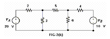
b. Using
Thevenin’s theorem find the current flowing through 5 ![]() resistor in the network of
FIG-2(b); (All resistances in
resistor in the network of
FIG-2(b); (All resistances in ![]() ) (10)
) (10)
Q.3 a. Derive an expression for conversion efficiency η of a full wave Bridge rectifier. Also show that ηmax in this case is 0.812. (8)
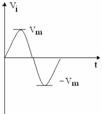
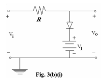
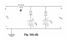
b. Input to the clipping circuits shown in FIG-3(b)(i) and FIG-3(b)(ii) is a sine wave of 10V peak; draw the output wave forms assuming ideal diodes and
|V1| =4V, |V2| = 2V. (8)
|
|

Q.4 a. Compare the performance of the 3 transistor configurations CE, CB and CC. (6)
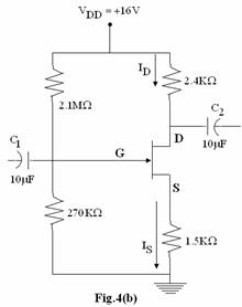
b. For
the JFET circuit shown in Fig. 4(b) find IDQ, VGSQ and VDSQ
if VP = -4V, IDSS= 8mA and VDD =
16V. (10)
Q.5 a. Derive an expression
for Stability factor ![]() of a biasing circuit. (8)
of a biasing circuit. (8)
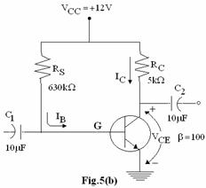
b. For the Fixed bias circuit shown in Fig 5(b), find the operating point ‘Q’ and stability factor ‘S’, assume for transistor VBE = 0.7V. (8)
|
Q.6 a. With a neat circuit diagram explain the role of each component in a RC coupled amplifier. Draw its frequency response and explain why the mid-band gain is constant? (12)
b. A Cascaded amplifier of 2 stages has A1 = 25 and A2 =10db. If Vi = 5mv, find Vo and the overall gain of the cascaded system in dB. (4)
Q.7 a. Classify the amplifiers based on the location of operating point (Q). Use suitable diagrams to explain. (8)
b. Prove that the maximum conversion efficiency of a Class-B power amplifier
is 78.5%. (8)
Q.8 a. What are the advantages of Negative feedback? Explain. (6)
b. Derive an expression for frequency of oscillation in an UJT relaxation oscillator. (10)
Q.9 a. Briefly explain the steps involved in IC fabrication. (8)
b. Calculate
the chip area needed for a 250 pF MOS capacitor given the thickness of SiO2
layer is 500 ![]() units and the relative dielectric
constant (εr) is 3.5. If the thickness of SiO2
layer is increased to 4.5, what is the new chip area and what is the percentage
change in area? (8)
units and the relative dielectric
constant (εr) is 3.5. If the thickness of SiO2
layer is increased to 4.5, what is the new chip area and what is the percentage
change in area? (8)