AMIETE – ET (OLD SCHEME)
 Code:
AE05 Subject:
BASIC ELECTRONICS
Code:
AE05 Subject:
BASIC ELECTRONICS
Time: 3 Hours Max. Marks: 100
NOTE: There are 9 Questions in all.
· Question 1 is compulsory and carries 20 marks. Answer to Q. 1. must be written in the space provided for it in the answer book supplied and nowhere else.
· Out of the remaining EIGHT Questions answer any FIVE Questions. Each question carries 16 marks.
· Any required data not explicitly given, may be suitably assumed and stated.
Q.1 Choose
the correct or the best alternative in the following: (2![]() 10)
10)
a. The Hall effect voltage in intrinsic silicon
(A) is positive.
(B) is zero.
(C) is negative.
(D) changes sign on application of magnetic field.
b. The main component responsible for lowering of gain in an R-C Coupled amplifier in Low Frequency range is
(A) Biasing system. (B) Resistor RE.
(C) Coupling capacitor CC. (D) Transistor itself.
c. A Source Follower using a FET usually has a voltage gain which is
(A) greater than +100. (B) slightly less than unity but positive.
(C) exactly unity but negative. (D) About -10.
d. Class-AB Operation is often used in Power (Large Signal) amplifiers in order to
(A) get maximum efficiency. (B) remove even harmonics.
(C) overcome cross-over distortion. (D) Reduce collector dissipation.
e. An Amplifier with no feedback has a gain-bandwidth product of 4 MHz. Its closed- Loop gain is 40. The new bandwidth is
(A) 100 KHz. (B) 160 MHz.
(C) 10 MHz. (D) 20 KHz.
f. Which of the following Oscillators is capable of giving highest Q-factor?
(A) Hartley Oscillator. (B) Tuned Oscillator
(C) Crystal Oscillator. (D) Wein-Bridge Oscillator.
g. The OP-AMP circuit shown
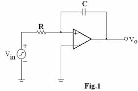
in Fig.1 is
(A) An Integrator.
(B) An Adder.
(C) A Differentiator.
(D) A Comparator.
h. The output time period of a transistorized monostable multivibrator using base resistor Rb and coupling capacitor Cb for the output transistor is given by
(A) Rb Cb (B) 0.69 Rb Cb.
(C) 2 Rb Cb (D) 1.38 Rb Cb.
i. If the output voltage of a Bridge Rectifier is 100 V, then the PIV of diode will be
(A)
![]()
![]() 100 V. (B)
100 V. (B)
![]() V.
V.
(C) ![]()
![]() 100 V. (D)
100 V. (D)
![]()
![]() 100 V.
100 V.
j. The gates required to build a Half-Adder are
(A) EX-OR Gate and NOR Gate.
(B) EX-OR Gate and OR Gate.
(C) EX-OR Gate and AND Gate.
(D) Four NAND Gates.
Answer any FIVE Questions out of EIGHT Questions.
Each question carries 16 marks.
Q.2 a. If the impurity content of either or both the P and the N-region is increased, what happens to the Potential Barrier, and why? Does the temperature affect the Potential Barrier? Explain. (8)
b. Define Transistor Characteristics. Sketch the Output Characteristics of a Transistor in its Common Base mode and explain the Active, Cut-off and Saturation Regions. Why CB configuration is rarely used in Audio-Frequency circuits? (8)
Q.3 a. A
CE transistor amplifier with h-parameters given by hie = 1100![]() , hre = 2.5
, hre = 2.5 ![]() 10-4 , hfe = 50, hoe = 25
10-4 , hfe = 50, hoe = 25 ![]() A/V. If RL = 1
K
A/V. If RL = 1
K![]() and RS = 1K
and RS = 1K![]() , then calculate (i) AI
(ii) RIN (iii) AV (iv) AVS (v) AIS (8)
, then calculate (i) AI
(ii) RIN (iii) AV (iv) AVS (v) AIS (8)
b. Draw the circuit of
Darlington Pair Amplifier and explain its operation. Also show that its current
gain is equal to![]() .Give its applications. (8)
.Give its applications. (8)
Q.4 a. Draw the Low Frequency model of a Source Follower Amplifier using FET and derive an expression for its voltage gain. (8)
b. A Transformer-Coupled Class-A Power Amplifier draws a current of 250 mA from a Collector supply of 12.5 V, when no signal is applied to it. Determine
(i) Maximum Output Power
(ii) Maximum Collector Efficiency and
(iii) Power rating of the transistor
If
the load connected across the transformer secondary is of 2![]() and transformer turn
ratio is 5:1, then comment on the Impedance Matching of this amplifier. (8)
and transformer turn
ratio is 5:1, then comment on the Impedance Matching of this amplifier. (8)
Q.5 a. The gain of an amplifier without feedback is 100 whereas with negative feedback it falls to 50. If due to ageing the amplifier gain falls to 80, find the Percentage reduction in stage gain (i) Without Feedback and (ii) With Negative Feedback. (6)
b. What is an Emitter Follower? Why is it so called? Draw the circuit diagram of an Emitter Follower using BJT and explain its working. Also show that this circuit Provides High Input Impedance and Low Output Impedance. (10)
Q.6 a. Calculate the Frequency of Oscillations when a
Phase-Shift Oscillator has R = 10 K![]() , C = 0.01
, C = 0.01 ![]() F and RC = 2.2
K
F and RC = 2.2
K ![]() .
What will be the minimum current gain needed for this purpose? (5)
.
What will be the minimum current gain needed for this purpose? (5)
b. Explain how a OP-AMP can be used to sum a number of input voltages applied to the Inverting terminal. How will you use the circuit to find the Average of Input Voltages? (7)
c. What do you mean by Input Offset Current in OP-AMP? What is its cause and how is it Minimized? (4)
Q.7 a. What is Schmitt Trigger and discuss its characteristic? How would you convert a Transistorized Bistable Multivibrator into Schmitt Trigger? (9)
b. Draw the circuit diagram
of Collector coupled Astable Multivibrator using NPN transistors and explain
its operation. Find the frequency and duty cycle of the Astable Multivibrator
Output, if R1 = 10K![]() , R2 = 5 K
, R2 = 5 K![]() and C1
= C2 = 0.1
and C1
= C2 = 0.1![]() F. (7)
F. (7)
Q.8 a. Draw
a neat circuit diagram of Transistor (Silicon) Shunt Voltage Regulator. Use the
following data in your circuit: VZ = 8.3 V, Vin = 22 V, RS
= 130![]() and RL = 100
and RL = 100![]() . Determine the (i) Regulated
Voltage and (ii) Collector current. Also give its drawbacks. (7)
. Determine the (i) Regulated
Voltage and (ii) Collector current. Also give its drawbacks. (7)
b. Draw the circuit of Centre-Tap Full Wave Rectifier using capacitor filter and explain its working by drawing input and output waveforms. (9)
Q.9 a. State and Prove De-Morgan’s Theorems. (5)
b. What is a Flip-Flop? What is the difference between a Latch and a Flip-Flop? (4)
c. What is an Asynchronous Counter? Draw the Logic Diagram of 3-bit Ripple Counter and explain its operation with the help of Timing Diagrams and Truth Table. (7)