AMIETE – CS/IT (OLD SCHEME)
 Code:
AC03 / AT03 Subject:
BASIC ELECTRONICS &
Code:
AC03 / AT03 Subject:
BASIC ELECTRONICS &
Time: 3 Hours DIGITAL CIRCUITS
Max. Marks: 100
NOTE: There are 9 Questions in all.
· Question 1 is compulsory and carries 20 marks. Answer to Q. 1. must be written in the space provided for it in the answer book supplied and nowhere else.
· Out of the remaining EIGHT Questions answer any FIVE Questions. Each question carries 16 marks.
· Any required data not explicitly given, may be suitably assumed and stated.
Q.1 Choose
the correct or the best alternative in the following: (2 ![]() 10)
10)
a. Which of the following will serve as donor impurity in silicon?
(A) Boron (B) Indium
(C) Germanium (D) Antimony
b. A BJT has a = 0.99, iB = IB= 25 μA and ICBO = 200 nA. The dc collector current will be-
(A) ≈ 2.5 mA (B) ≈ 5 mA
(C) 250 mA (D) 5 mA
c. If the inputs to the circuit shown in figure are A and B the output f can be represented as
|
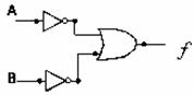
(A) Two input NAND gate
(B) Two input NOR gate
(C) Two input XOR gate
(D) None
d. In a Wien bridge oscillator with R = 5 K and C = 0.01 μF, the frequency of oscillation will be
(A) 7.8 kHz (B) 3.2 kHz
(C) 2.5 kHz (D) 780 Hz
![]()
e. The enhancement type N-Channel MOSFET is
represented by symbol
![]()
(A) (B)
![]()
![]()
![]() (C) (D)
(C) (D)
![]()
f. If the differential and common mode gains of a differential amplifier are 60 and 0.3 respectively, then the CMRR will be
(A) 20 (B) 200
(C) 18 (D) 2000
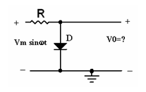
g. Maximum rectifying efficiency of half wave rectifier (without a filter circuit) is
(A) 0.812 (B) 1.1
(C) 0.604 (D) 0.406
h. Which of the following is a unipolar device?
(A) p-n junction diode (B) Zener diode
(C) Tunnel diode (D) Schottky diode
i. The voltage gain of the Darlington amplifier is
(A) equal to unity (B) less than unity
(C) greater than unity (D) equal to zero
j. The decimal equivalent of the hexadecimal number (BAD)16 is
(A) 111013 (B) 5929
(C) 3416 (D) 2989
Answer any FIVE Questions out of EIGHT Questions.
Each question carries 16 marks.
Q.2 a. What are intrinsic and extrinsic semiconductors? Illustrate with proper diagram and examples. (4)
b. Draw and explain the ideal diode characteristics and large signal diode models in forward and reverse biased condition. (6)
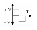
c. Draw the outputs waveforms for each of the following circuits: (6)
Q.3 a. Why is it preferable to express amplifier gain on a logarithmic scale than on a linear scale? Draw a neat diagram of two-stage RC coupled amplifier along with is frequency response. Derive the expression for its current / voltage gain in mid frequency region. (8)
b. State the limitations of transistor h-parameters. (2)
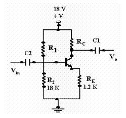
c. Given that ICQ = 2 mA, VCEQ = 10 V, Vcc = 18 V, RE=1.2 K,R2= 18 K, VBE = 0.7 V
Determine R1 and RC for the network shown below: (6)
Q.4 a. With neat diagram briefly explain the following for n-channel JFET-
(i) Volt- Ampere characteristics. (Drain characteristics)
(ii) Transfer characteristics. (6)
b. Explain the operation of FET as a switch. (4)
c. How oscillators are different from amplifiers? State the Barkhausen criterion for oscillations and explain the operation of crystal oscillator. (6)
Q.5 a. With neat circuit derive output voltage expressions for Op-amp as differentiator and an integrator. (6)
b. From the characteristics of Op-amp, define the terms-
(i) Input offset voltage(ii) Slew rate (2)
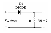
c. In a full wave rectifier the load resistance is RL = 2 K. Each diode has idealized characteristics having slope corresponding to a resistance of 400 Ω. Voltage applied to each diode is 240sin50t. Find
(i) Peak value of current
(ii) DC or average value of current
(iii) RMS value of current
(iv) Rectifier efficiency
(v) Ripple factor
List three disadvantages of half wave rectifier. (8)
Q.6 a. Simplify the Boolean expression ![]() together with don’t
care conditions d in (i) sum of products (ii)Product
of Sums
together with don’t
care conditions d in (i) sum of products (ii)Product
of Sums
![]() and
and ![]() (6)
(6)
b. Realize a full subtractor logic circuit with two half subtractors and OR gate.
(4)
c. A combinational circuit is defined by function ![]() and
and ![]() . Implement the circuit
using PLA.
. Implement the circuit
using PLA.
![]()
![]() (6)
(6)
Q.7 a. Draw the circuit for a CMOS NOR gate and briefly explain. (6)
b. Sketch the NMOS inverter circuits with saturated enhancement load, linear load and NMOS depletion load. Comment on the transfer characteristics in each case. (10)
Q.8 a. Describe briefly fundamental applications of counter. (4)
b. What is race around condition in JK flip-flop? Draw the circuit with truth table to convert JK flip-flop to D flip-flop. (8)
c. List the advantages of synchronous counters over ripple counters. (4)
Q.9 a. Sketch the circuit of a 4-NMOS dynamic RAM cell and briefly explain its operation. Compare it with 6-NMOS cell RAM circuit. (8)
b. What determines minimum and maximum frequency of operation of CCD? (4)
c. Draw the block diagram of microcomputer and state how does microcomputer differ from microprocessor? List applications of microprocessors. (4)