Code: DE09 Subject: DIGITAL ELECTRONICS
Time: 3 Hours Max. Marks: 100
NOTE: There are 9 Questions in all.
· Question 1 is compulsory and carries 20 marks. Answer to Q. 1. must be written in the space provided for it in the answer book supplied and nowhere else.
· Out of the remaining EIGHT Questions answer any FIVE Questions. Each question carries 16 marks.
· Any required data not explicitly given, may be suitably assumed and stated.
Q.1 Choose the correct or best alternative in the following: (2x10)
a. The 2’s complement of the number 1101110 is
(A) 0010001. (B) 0010001.
(C) 0010010. (D) None.
b. The digital logic family which has the lowest propagation delay time is
(A) ECL (B) TTL
(C) CMOS (D) PMOS
c. The decimal equivalent of Binary number 10101 is
(A) 21 (B) 31
(C) 26 (D) 28
d. How many two input AND gates and two input OR gates are required to realize Y = BD+CE+AB
(A) 1, 1 (B) 4, 2
(C) 3, 2 (D) 2, 3
e. How many select lines will a 32:1 multiplexer will have
(A) 5. (B) 8.
(C) 9. (D) 11.
f. How many address bits are required to represent 4K memory
(A) 5 bits. (B) 12 bits.
(C) 8 bits. (D) 10 bits.
g. For JK flipflop J = 0 K=1, the output after clock pulse will be
(A) 1. (B) no change.
(C) 0. (D) high impedance.
h. Which of following are known as universal gates
(A) NAND & NOR. (B) AND & OR.
(C) XOR & OR. (D) None.
i. Which of the following memories stores the most number of bits
(A) ![]() memory.
(B)
memory.
(B) ![]() memory.
memory.
(C) ![]() memory.
(D)
memory.
(D) ![]() memory.
memory.
j. Which of following consume minimum power
(A) TTL. (B) CMOS.
(C) DTL. (D) RTL.
Answer any FIVE Questions out of EIGHT Questions.
Each question carries 16 marks.
Q.2 a. Convert ![]() to
octal.
(8)
to
octal.
(8)
b. Perform the following subtraction using 1’s complement
(i) 11001 – 10110 (ii) 11011 - 11001 (8)
Q.3 a. Prove the following identities
(i) ![]()
(ii) ![]() (8)
(8)
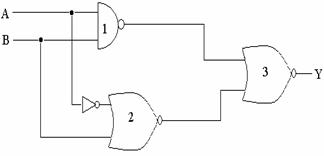
b. Find the boolean expression for the logic circuit shown
below.
(8)
|
Q.4 a. Reduce the following equation using k-map
![]() (8)
(8)
b. Describe CMOS inverter and state advantages of CMOS. (8)
Q.5 a. Implement the following function using 8 to 1 multiplexer
![]() (8)
(8)
b. What is parallel adder? Draw and explain block diagram for 4 bit parallel adder. (8)
Q.6 a. What is parity generator and checker? Describe five bit even parity checker. (8)
b. Describe interfacing of CMOS to TTL. (8)
Q.7 a. Describe the operation of parallel in parallel out (PIPO) shift register. (8)
b. Design a mod-12 asynchronous up counter. (8)
Q.8 a. (i)
How many ![]() RAM chips are required to
provide a memory capacity of 2048 bytes.
RAM chips are required to
provide a memory capacity of 2048 bytes.
(ii) How many lines of address bus must be used to access 2048 bytes of memory. How many lines of these will be common to each chip?
(iii) How many bits must be decoded for chip select? What is the size of decoder? (8)
b. Describe basic dynamic MOS RAM cell. (8)
Q.9 a. How many bits are required at the input of a ladder D/A converter, if it is required to give a resolution of 5mV and if the full scale output is +5V. Find the %age resolution. (8)
b. Describe the operation of voltage to frequency ADC. (8)