 Code: DE08 Subject: ANALOG ELECTRONICS
Time: 3 Hours Max. Marks: 100
NOTE: There are 9 Questions in all.
· Question 1 is compulsory and
carries 20 marks. Answer to Q. 1. must be written in the space provided for it
in the answer book supplied and nowhere else.
· Out of the remaining EIGHT
Questions answer any FIVE Questions. Each question carries 16 marks.
· Any required data not
explicitly given, may be suitably assumed and stated.
Q.1 Choose
the correct or best alternative in the following: (2x10)
a. A semiconductor has a
(A)
negative temperature co-efficient of resistance.
(B) positive temperature co-efficient of
resistance.
(C) constant temperature
co-efficient of resistance.
(D) None
of above.
b. When a p-n
junction is reverse biased
(A)
the
width of depletion layer increases.
(B)
it
offers high resistance.
(C)
small
current flows through it.
(D)
All
of above.
c. For faithful amplification with germanium
transistor, the base emitter junction voltage ![]() should not fall below
should not fall below
(A) 0.3 V (B) 0.5 V
(C) 0.7 V (D) 0.1 V
d. The ideal value of stability factor is
(A) 1 (B) 5
(C) 10 (D) 100
e. A high Q tuned circuit in an amplifier permits it to have high
(A) selectivity. (B) fidelity.
(C) sensitivity. (D) frequency range.
f. The final stage of an amplifier uses
(A)
R-C
coupling. (B) transformer coupling.
(C) direct coupling. (D) all of above.
g. A push pull amplifier
(A) reduces odd harmonics in
output.
(B) reduces even harmonics in
output.
(C)
is
the first stage of an audio amplifier.
(D)
uses
single transistor.
h. The voltage gain of an amplifier is 100. When negative feedback with a factor of 0.04 is introduced, its gain will be
(A) 20 (B) 25
(C) 4 (D) 0.4
i. The loop gain of the oscillator to start with is
(A) more than 100 (B)
slightly more than 1
(C)
less than 1 (D)
none of above
j. The gain of op-amp decreases at high frequency because of
(A) external capacitance. (B)
external resistance.
(C) internal capacitance. (D) internal resistance.
Answer
any FIVE Questions out of EIGHT Questions.
Each
question carries 16 marks.
Q.2 a. Describe the self bias method of biasing for
BJT. (8)
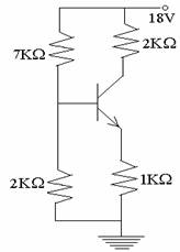
b. For voltage
divider biasing circuit given below, find emitter current, collector emitter
voltage and collector voltage. (8)

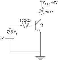
Q.3 a. Find the D.C. voltages and currents for the
silicon n-p-n transistor given below assuming

![]() . Determine the small
signal model and voltage gain of the amplifier. (10)
. Determine the small
signal model and voltage gain of the amplifier. (10)
b. Explain how MOSFET is biased using self
bias method. (6)
Q.4 a. Derive an expression for efficiency of class-A amplifier. Show that its maximum value is 50%. (8)
b. For a power
amplifier working in class A operation, the zero signal collector current is
100 mA. If dc supply voltage ![]() .
.
Find
(i) the maximum ac power output
(ii) power
rating of transistor
(iii) the
maximum collector efficiency. (8)
Q.5 a. An
amplifier has gain A = 60dB and output impedance ![]() . It is required to
modify its output impedance to
. It is required to
modify its output impedance to ![]() by negative
feedback. Find
by negative
feedback. Find
(i) value of feedback factor.
(ii) the percentage change in overall gain for 10% change in gain of basic amplifier. (8)
b. What do you mean by feedback?
Derive an expression for gain with feedback. (8)
Q.6 a. Explain the characteristics of an ideal
op-amp. (8)
b. Draw the circuit diagram of second order low pass
Butterworth filter and derive an expression for cut off frequency. (8)
Q.7 a. Describe the process of square wave
generation using op-amp. (8)
b. Describe the operation of 555 timer as an
astable multivibrator. (8)
Q.8 a. Draw the circuit of shunt biased negative
clipper and explain its working, when the input waveform is 20V (peak to peak)
and a biasing voltage of 7V. Draw output
waveform. (8)
b. Draw and
explain the working of UJT relaxation oscillator. (8)
Q.9 a. In a transistor Hartley oscillator if ![]() ,
, ![]() and mutual inductance
between two coils
and mutual inductance
between two coils ![]() . Calculate value of
capacitor
. Calculate value of
capacitor ![]() of oscillatory circuit
to obtain frequency of 4110 kHz. (8)
of oscillatory circuit
to obtain frequency of 4110 kHz. (8)
b. Explain the operation of FET as an
amplifier. State its advantages. (8)