 Code: DE06 Subject:
BASIC ELECTRONICS
Code: DE06 Subject:
BASIC ELECTRONICS
Time: 3 Hours Max. Marks: 100
NOTE: There are 9 Questions in all.
· Question 1 is compulsory and
carries 20 marks. Answer to Q. 1. must be written in the space provided for it
in the answer book supplied and nowhere else.
· Out of the remaining EIGHT
Questions answer any FIVE Questions. Each question carries 16 marks.
· Any required data not
explicitly given, may be suitably assumed and stated.
Q.1 Choose
the correct or best alternative in the following: (2x10)
a. The colour band sequence of a
resistor is Yellow, Violet,
(A) ![]() and
and ![]() (B)
(B) ![]()
![]() and
and ![]()
![]()
(C) ![]() and
and ![]() (D)
(D) ![]() and
and ![]()
b. With increasing temperature, the resistivity of an intrinsic semiconductor decreases. This is because, with the increase of temperature
(A)
The
carrier concentration increases but the mobility of carriers decreases.
(B) Both the carrier
concentration and mobility of carriers decreases.
(C) The
carrier concentration decreases, but the mobility of carriers increases.
(D) The
carrier concentration remains the same but the mobility of carriers decreases.
c. At room temperature of 25ºC, the barrier Potential for Silicon is 0.7V. Its value at 0ºC will be
(A)
0.7 V. (B) 0.65 V.
(C) 0.75 V. (D) 0.55 V.
d. Which of the following is a unipolar device?
(A) P-N junction diode (B)
Zener diode
(C) Tunnel diode (D) Schottky diode
e. On applying a Positive voltage signal to the base of a normally biased N-P-N CE transistor amplifier
(A) Base current will fall.
(B) Collector current will fall.
(C) Emitter current will fall.
(D) Collector voltage will become less positive.
f. An N-channel JFET has Pinch-off Voltage of VP = – 4V and given that VGS = –1V, then the minimum VDS for the device to operate in the Pinch-off region will be
(A) +1V (B) +3V
(C) +4V (D) +5V
g. The extremely high input impedance of a MOSFET is Primarily because of
(A) Absence of its channel
(B) Depletion of current carriers
(C) Extremely small leakage current of its gate
capacitor
(D) Negative VGS
h. When two identical SCRs are placed back-to-back in series with a load and if each is fired at 90º, then the voltage across the load will be
(A) ![]() (B) Zero
(B) Zero
(C) ![]() (D)
(D) ![]()
i. The most commonly used type of electron emission in electron tubes is
(A) Photo-electron emission. (B) Thermionic emission.
(C) Field emission. (D) Secondary emission.
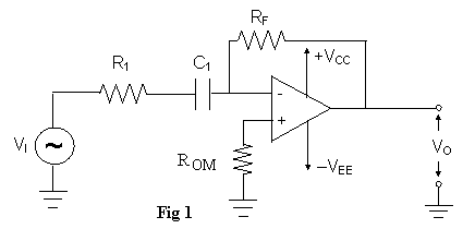 j. In the
differentiating circuit shown in Fig.1, the function of resistor R1
is to
j. In the
differentiating circuit shown in Fig.1, the function of resistor R1
is to
(A)
Enable
the circuit to approach ideal differentiator
(B) Maintain high input impedance
(C) Eliminate high frequency
noise spikes
(D) Prevent oscillations at high
frequencies
Answer any FIVE Questions out
of EIGHT Questions.
Each question carries 16
marks.
Q.2 a. What is an inductor? Explain briefly various
types of fixed inductors employed in electronic industry. What is the role of
variable inductors in radio receiver? (6)
b. Differentiate
between a current source and a voltage source. Give their graphical
representations. How can they be converted from one another? Determine the
current flowing through 7Ω resistor in the circuit shown in Fig. 2 by
using source transformation technique. (10)
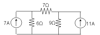
Fig 2
Q.3 a. “As regards conduction of current in
concerned, a semiconductor is bipolar in nature whereas a metal is
unipolar”-Justify (or) nullify the above statement. (7)
b. Explain what do you understand by intrinsic,
N-type and P-type semiconductors. Discuss the position of Fermi level in each
case (9)
Q.4 a. Discuss
the reasons for the existence of a depletion layer in a P-N junction. Relate it
to the rectifying properties of a P-N junction. (10)
b. What is a Zener diode? Explain, with the help
of a circuit diagram. How Zener diode can be used as a voltage regulator? (6)
Q.5 a. Explain the operation of JFET as an analog switch. (7)
b. Compare the characteristics of CB, CE and CC configurations of a
transistor. Draw the circuit of a common collector transistor configuration and
explain its operation. Also derive the relation between ![]() and α current
amplification factors. (9)
and α current
amplification factors. (9)
Q.6 a. Explain with a diagram the operation of
Positive adjustable voltage regulator and derive an expression for output
voltage. (9)
b. In a centre-tap full-wave rectifier, the load
resistance RL=1KΩ. Each diode has a forward-bias dynamic
resistance rd of 10Ω. The voltage across half the secondary
winding is ![]() Find
Find
(i) the Peak value of current
(ii) the dc or average value of current
(iii) the rms value of current
(iv) the ripple factor and
(v)
the rectification efficiency (7)
Q.7 a. Why are MOSFETs available in both enhancement
and depletion modes, while JFETs operate almost invariably in the depletion
modes. (4)
b. Sketch the output characteristics for
N-channel JFET with gate-source voltage shorted (i.e. VGS=0). How
Ohmic, Pinch-off and Breakdown regions are created? (8)
c. For an
N-channel JFET, IDSS = 8.7mA, VP = –3V and VGS =
–1V, then find the value of drain current (ID). (4)
Q.8 a. Describe
the structure, symbol and operation of SCR with the help of suitable diagrams. (8)
b. What is
monolithic IC? Explain photolithographic Process in monolithic IC Production. (8)
Q.9 a. Explain the following terms as referred to an
operational amplifier
(i)
Input offset Voltage
(ii)
Input offset Current
(iii)
Slew Rate
(iv)
CMRR (12)
b. An operational amplifier shown in Fig.3 has
feedback resistor Rf = 12 KΩ and the resistances in the
input sides are RS1=12KΩ, RS2=2KΩ and RS3=3KΩ. The
corresponding inputs are Vi1
= +9V, Vi2 = –3V
and
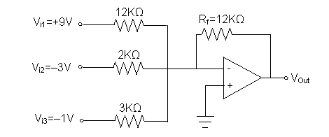 Vi3 = –1V. Non-inverting terminal is
grounded. Calculate the output voltage. (4)
Vi3 = –1V. Non-inverting terminal is
grounded. Calculate the output voltage. (4)