Code: DC02 Subject: FUNDAMENTALS OF ELECTRONICS
Time: 3 Hours Max. Marks: 100
NOTE: There are 9 Questions in all.
· Question 1 is compulsory and carries 20 marks. Answer to Q. 1. MUST BE WRITTEN IN THE SPACE PROVIDED FOR IT in the answer book supplied and nowhere else.
· Out of the remaining EIGHT Questions answer any FIVE Questions. Each question carries 16 marks.
· Any required data not explicitly given, may be suitably assumed and stated.
Q.1 Choose the correct or best alternative in the following: (2x10)
a. If the colour code on the body of a resistor is Brown, Black, Blue and Silver then the value of the resistance is
(A) ![]() (B)
(B) ![]()
(C) ![]() (D)
(D) ![]()
b. The short circuit current for a voltage source with an open circuit voltage of 12V and an internal resistance of 3 ohms is
(A) 2 A (B) 2 mA
(C) 4 A (D) 5.2 A
c. An impurity atom like boron when added to a pure crystal of germanium results in
(A) an intrinsic semiconductor (B) an N-type doped semiconductor
(C) a P-type doped semiconductor (D) a junction diode
d. A diode that has no depletion layers and which operates with hot carriers is called a
(A) Gunn diode (B) Step recovery diode
(C) Schottky diode (D) Varactor diode
e. A tunnel diode is
(A) a very heavily-doped PN junction diode.
(B) a high resistivity PN junction diode.
(C) a slow switching device.
(D) used with reverse bias.
f. The mid frequency gain of an amplifier is 100 for a bandwidth of 200 KHz with 5% negative feedback introduced to the above amplifier, its new bandwidth will be
(A) 250 KHz (B) 2500 KHz
(C) 3300 KHz (D) 1200 KHz
g. The Boolean expression ‘Y’ for the logic circuit shown below in Fig.1 is
|
|
|
|
|
|
|
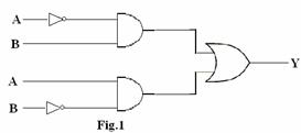
(A) ![]()
(B) ![]()
(C)
![]()
(D)
![]()
h. Noise margin of digital logic families is expressed in
(A) decibel (B) watt
(C) volt (D) degree kelvin
i. The feedback path in an OPAMP integrator consists of
(A) a resistor
(B) a capacitor
(C) a resistor and a capacitor in series
(D) a resistor and a capacitor in parallel
j The most important application of IC is in
(A) high power circuits (B) simple circuits
(C) computers (D) none of the above
Answer any FIVE Questions out of EIGHT Questions.
Each question carries 16 marks.
Q.2 a. What do you mean by a passive circuit component? What is an “Inductor”? What are its uses? Name the types of inductors. (7)
b. What are voltage and current sources? Write in brief about the internal resistance of a source. (6)
c. State Thevenin’s theorem and Norton’s theorem. (3)
Q.3 a. What do you mean by “doping” as used in semiconductor theory and what is its effect? Define N-type and P-type semiconductors. Give examples for the type of doping elements that can be used to obtain them. (6)
b. How do you obtain a semiconductor diode? Define the quantity “dynamic forward resistance” for a semiconductor diode. Explain briefly how this quantity can be obtained using the V-I characteristics for the diode. What do you mean by dynamic reverse resistance of the diode? (7)
c. An ideal diode is supplying current to a 6 ohm resistor when it is forward biased by a power supply of 12 V. Calculate the circuit current and power dissipated in the ideal diode. (3)
Q.4 a. What is a liquid crystal? Briefly describe a LCD eight-segment digit display. Comment on the speed of operation of LCDs as compared to LEDs. What is the distinct advantage of LCD? (8)
b. A Zener diode is rated as a 500-mW, 20% diode. If the Zener voltage for the diode is specified as “Nominal, 10V” by the manufacturer, comment on the variation of the Zener potential in its range of application. (3)
c. Briefly explain the following for a Schottky diode:
(i) Its construction.
(ii) Its action under zero bias condition. (5)
Q.5 a. What is a transistor? Write the graphic symbol of a transistor and comment. (4)
b. Illustrate and briefly explain the input characteristics and output characteristics for a common-base silicon transistor circuit. (12)
Q.6 a. What are the basic elements of a feedback amplifier? Write the features of the following:
(i) Series feedback connections
(ii) Shunt feedback connections
(iii) Voltage feedback
(iv) Current feedback (7)
b. What does MOSFET represent? How do you compare JFET with MOSFET? Which are the types of MOSFETs commonly used? (6)
c. Name three typical applications of FET. (3)
Q.7 a. Demonstrate how NAND gates can be used to obtain the following:
(i) OR logic.
(ii) AND logic.
(iii) NOT logic. (6)
b. What is a logic gate? Write the circuit symbol and the truth tables for the following logic gates:
(i) The two-input NOR gate.
(ii) The two-input NAND gate.
Illustrate how two-input NOR gates can be used to realise a two-input AND gate. (6)
c. Define a standard POS Boolean expression, convert the given Boolean expression into a standard POS form. Write the steps to be followed.
![]() (4)
(4)
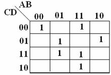
Q.8 a. Write a
brief note on Karnaugh map. A Karnaugh map is shown below. Write
the logical equation in the standard POS
form.
(7)
|
b. A four-variable logic function is given by,

Minimize the above function using K-map. (5)
c. Write the circuit of a TTL gate with totem-pole output driver. What is the reason behind including totem-pole output driver for the basic TTL gate? (4)
Q.9 a. What is the order of Fan-out for MOS logic? Give reasons for your answer. How is a CMOS obtained? Write the circuit of a two-input CMOS NAND gate and its truth table indicating the states of the MOS devices used. (8)
b. What are the ideal characteristics of an op-amp. (5)
c. What is an integrated circuit? Write two disadvantages of integrated circuits. (3)