Code: AE09 Subject: ANALOG & DIGITAL ELECTRONICS
Time: 3 Hours Max. Marks: 100
NOTE: There are 9 Questions in all.
· Question 1 is compulsory and carries 20 marks. Answer to Q. 1. must be written in the space provided for it in the answer book supplied and nowhere else.
· Out of the remaining EIGHT Questions answer any FIVE Questions. Each question carries 16 marks.
· Any required data not explicitly given, may be suitably assumed and stated.
Q.1 Choose the correct or best alternative in the following: (2x10)
a. The large signal differential voltage amplification of the 741 OPAMP is typically about
(A) 100 V/mv. (B) 500 V/mv.
(C) 1000 V/mv. (D) 200 V/mv.
b. If the input offset current and the average input bias current for an OPAMP are respectively 5nA and 30 nA, then the input bias currents at each input of the OPAMP are respectively
(A) 32.5 nA & 27.5 nA. (B) 22.5 nA & 30.2 nA.
(C) 10 nA & 16 nA. (D) 2.5 nA & 3.02 nA.
c. In a first-order low-pass active filter, if the values of the
resistance and the capacitor used are 1.2 ![]() and
and ![]() respectively,
then the cut-off frequency of the filter is
respectively,
then the cut-off frequency of the filter is
(A) 3.6 KHz. (B) 8.7 KHz.
(C) 8.2 Hz. (D) 6.63 KHz.
d. A clock rate of one megahertz operating a 12-stage counter of a counter-type ADC would need a maximum conversion time of approximately
(A) 3.2 ms. (B) 4.1 ms.
(C) 8 ms. (D) 7.1 ms.
e. Typical propagation delay of an ECL circuit is
(A) 10 ns. (B) 5 ns.
(C) 1 ns. (D) 3.2 ns.
f. The number of states in its counting sequence that a ring counter consisting of ‘n’ flip-flops can have is
(A) ![]() (B)
(B) ![]()
(C) ![]() (D)
(D) ![]()
g. The number of select input lines required by a 1-to-8 demultiplexer are
(A) Two. (B) One.
(C) Four. (D) Three.
h. The Maximum binary number counted by a ripple counter that uses form FFs is
(A) ![]() (B)
(B) ![]()
(C)
![]() (D)
(D) ![]()
i. The cut-in voltage of the aluminium n-type Schottky diode is about
(A) 0.5
V.
(B) 0.5 ![]() .
.
(C) 0.35 V. (D) 0.35 mV.
j. In applications where measurement of a physical quantity is involved, the OPAMP circuit recommended is
(A) Basic non-inverting amplifier. (B) A comparator.
(C) An active filter. (D) An instrumentation amplifier.
Answer any FIVE Questions out of EIGHT Questions.
Each question carries 16 marks.
Q.2 a. What is it that an OPAMP contains to achieve a very high voltage gain? What do you mean by common-mode rejection as applied to an OPAMP? (4)
b. With a circuit for illustration, explain the effect of the input
offset voltage for the OPAMP, ![]() (which is normally specified in
the manufacturer’s data sheet) on the
output.
(7)
(which is normally specified in
the manufacturer’s data sheet) on the
output.
(7)
c. Write a note on frequency response of OPAMPS. (5)
Q.3 a. What is the role of an OPAMP in an active filter? Define an ideal low-pass filter. Write the equation for the squared magnitude response of a low-pass Butterworth filter. Mention the variables involved in the above equation. (7)
b. Design a first order high-pass active filter for a cut-off frequency of 10 KHz providing a pass-band gain of 1.5. Illustrate the circuit of the filter designed and find the magnitude of the response for the following frequencies:
(i) 10 Hz (ii) 100 Hz
(iii) 500 Hz (iv) 1000 Hz (9)
Q.4 a. Starting from fundamentals, explain the meaning of the term “SWITCHING TIME” as applied to a semiconductor diode. What is the use of the above quantity? (8)
b. What is the advantage of Schottky diode over an ordinary PN-junction diode in terms of speed of operation? Support your answer with relevant comments. (4)
c. What are the advantages of switched capacitor filters? (4)
Q.5 a. What is an ADC? Compare the performance of a flash ADC with successive approximation ADC. (6)
b. For the OPAMP circuit shown in the Fig.1, show that the output will be proportional to the logarithm of the input voltage. (10)
|
|
|
|
|
|
|
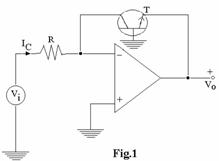
Comment on the disadvantage of the circuit, if any.
Q.6 a. What are NMOS and PMOS logic circuits? Write the circuit of an NMOS nor-gate and briefly explain. (7)
b. Write a note on a ROM with an illustration. (9)
Q.7 a. What are the important elements of a bipolar IC? How are bipolar logic circuits broadly classified? Give examples for each classification. (8)
b. What is the other name given to the ECL family? Comment on your answer. What are the characteristics of ECL family? (8)
Q.8 a. What is a digital magnitude comparator? With a circuit diagram that uses exclusive-NOR gate, AND gates and inverters, explain the operation of a single-bit magnitude comparator. (7)
b. Write the general structure of a PLA. Write the logic
diagram of a general ![]() PLA. How are PLAs characterised?
(6)
PLA. How are PLAs characterised?
(6)
c. Write the logic diagram, Truth table, and the logic symbol of a positive-edge-triggered T flip-flop. (3)
Q.9
a. Design a combinational circuit that
accepts a 3-bit number as input and generates an output binary number equal to
the square of the input number using
b. What is a counter? How are counters broadly classified? Write at least two lines on each such classification. (7)