Code: AE05 Subject: BASIC ELECTRONICS
Time: 3 Hours Max. Marks: 100
NOTE: There are 9 Questions in all.
· Question 1 is compulsory and carries 20 marks. Answer to Q. 1. must be written in the space provided for it in the answer book supplied and nowhere else.
· Out of the remaining EIGHT Questions answer any FIVE Questions. Each question carries 16 marks.
· Any required data not explicitly given, may be suitably assumed and stated.
Q.1 Choose the correct or best alternative in the following: (2x10)
a. In an intrinsic semiconductor, the Fermi level is
(A) closer to the valence band
(B) midway between conduction and valence band
(C) closer to the conduction band
(D) within the valence band
b. The reverse saturation current of a silicon diode
(A) doubles for every 10°C increase in temperature
(B) does not change with temperature
(C) halves for every 1°C decrease in temperature
(D) increases by 1.5 times for every 2°C increment in temperature
c. The common collector amplifier is also known as
(A) collector follower (B) Base follower
(C) Emitter follower (D) Source follower
d. In class A amplifier, the output current flows for
(A) a part of the cycle or the input signal.
(B) the full cycle of the input signal.
(C) half the cycle of the input signal.
(D) 3/4th of the cycle of the input signal.
e. In an amplifier with negative feedback,
(A) only the gain of the amplifier is affected
(B) only the gain and bandwidth of the amplifier are affected
(C) only the input and output impedances are affected
(D) All of the four parameters mentioned above would be affected
f. Wien bridge oscillator can typically generate frequencies in the range of
(A) 1KHz – 1MHz
(B) 1 MHz – 10MHz
(C) 10MHz – 100MHz
(D) 100MHz – 150MHz
g. A differential amplifier, amplifies
(A) and mathematically differentiates the average of the voltages on the two input lines
(B) and differentiates the input waveform on one line when the other line is grounded
(C) the difference of voltages between the two input lines
(D) and differentiates the sum of the two input waveforms
h. The transformer utilization factor of a half-wave rectifier is approximately
(A) 0.6 (B) 0.3
(C) 0.9 (D) 1.1
i. The dual of the Boolean expression: ![]() is
is
(A) ![]() (B)
(B) ![]()
(C) ![]() (D)
(D) ![]()
j. It is required to construct a counter to count upto 100(decimal). The minimum number of flip-flops required to construct the counter is
(A) 8 (B) 7
(C) 6 (D) 5
Answer any FIVE Questions out of EIGHT Questions.
Each question carries 16 marks.
Q.2 a. Describe how conductivity and carrier mobility of a sample of semiconductor can be determined by subjecting it to Hall effect. (8)
b. Draw the symbol and characteristics of a N-channel JFET and mark linear region, saturation region and breakdown region. (8)
Q.3 a. Using necessary circuits and waveforms illustrate and explain positive and negative clamping of voltages. (12)
b. A load line intersects the forward V-I characteristic of a silicon diode at Q, where the slope of the curve is 40mA/V. Calculate the diode resistance at the point Q. (4)
Q.4 Draw the circuit of a RC-coupled amplifier. Explain its behaviour at low-, mid- and high-frequencies by drawing separate equivalent circuit for each frequency region. (16)
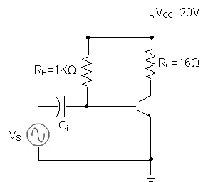
Q.5 a. The power amplifier shown below is operated in class A, with a base current drive of 8.5mA peak. Calculate the input dc power, the power dissipated in the transistor, the signal power delivered to the load and the overall efficiency of the amplifier, if transistor β=30 and VBE=0.7V. (8)
|
|
|
|
|
|
b. Derive mathematical expressions to illustrate the effects of negative feedback (i) to improve gain stabilization (ii) to reduce distortion (iii) to modify input and output impedances. (8)
Q.6 a. Write the circuit of clapp oscillator and explain its operation. What is its distinct advantage over other tuned oscillators? (7)
b. Explain how opamp can be used as a
(i) Differentiator (ii) Integrator
(iii) Inverting amplifier (9)
Q.7 a. Draw the circuit of a sawtooth generator and explain its operation in detail. (12)
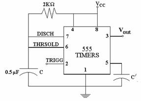
b. Find the period of the output pulse in the circuit shown below: (4)
|
|
|
|
|
|
|
Q.8 a. Analyze half-wave and full-wave rectifier circuits (without filter) to deduce the values of rectification efficiency assuming ideal diodes. (8)
b. Explain the operation of a foldback current-limiting circuit connected to a series voltage regulator, by drawing a neat circuit diagram. (8)
Q.9 a. Prepare the truth-table for the function
ƒ(a,
b, c) = ![]()
Minimize the function using K-map. Draw the logic diagram using gates of your choice to realize the minimized function. (8)
b. Construct a 4-bit ripple counter for binary counting, using JK flip-flops and describe its operation with the help of timing diagrams. (8)