Code: AC07/AT07 Subject: COMPUTER ARCHITECTURE
Time: 3 Hours Max. Marks: 100
NOTE: There are 9 Questions in all.
· Question 1 is compulsory and carries 20 marks. Answer to Q. 1. must be written in the space provided for it in the answer book supplied and nowhere else.
· Out of the remaining EIGHT Questions answer any FIVE Questions. Each question carries 16 marks.
· Any required data not explicitly given, may be suitably assumed and stated.
Q.1 Choose the correct or best alternative in the following: (2x10)
a. Which of the following is a self complementing code?
(A) 8421 code (B) 5211
(C) Gray code (D) Binary code
b. Which gate can be used as anti-coincidence detector?
(A) X-NOR (B) NAND
(C) X-OR (D) NOR
c. Which of the following technology can give high speed RAM?
(A) TTL (B) CMOS
(C) ECL (D) NMOS
d. In 8085 microprocessor how many I/O devices can be interfaced in I/O mapped I/O technique?
(A) Either 256 input devices or 256 output devices.
(B) 256 I/O devices.
(C) 256 input devices & 256 output devices.
(D) 512 input-output devices.
e. After reset, CPU begins execution of instruction from memory address ___________.
(A) ![]() (B)
(B) ![]()
(C)
![]() (D)
(D) ![]()
f. Which is true for a typical RISC architecture?
(A) Micro programmed control unit.
(B) Instruction takes multiple clock cycles.
(C) Have few registers in CPU.
(D) Emphasis on optimising instruction pipelines.
g. When an instruction is read from the memory, it is called
(A) Memory Read cycle (B) Fetch cycle
(C) Instruction cycle (D) Memory write cycle
h. Which activity does not take place during execution cycle?
(A) ALU performs the arithmetic & logical operation.
(B) Effective address is calculated.
(C) Next instruction is fetched.
(D) Branch address is calculated & Branching conditions are checked.
i. A circuit in which connections to both AND and OR arrays can be programmed is called
(A) RAM (B) ROM
(C) PAL (D) PLA
j. If a register containing data ![]() is
subjected to arithmetic shift left operation, then the content of the register
after ‘ashl’ shall be
is
subjected to arithmetic shift left operation, then the content of the register
after ‘ashl’ shall be
(A) ![]() (B)
(B) ![]()
(C) ![]() (D)
(D) ![]()
Answer any FIVE Questions out of EIGHT Questions.
Each question carries 16 marks.
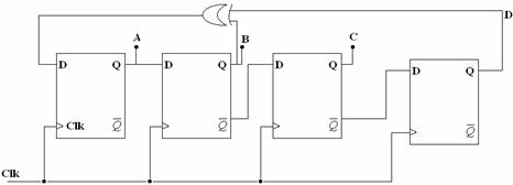
Q.2 a. Consider the following circuit consisting of four D-FF and an EX-OR gate. The initial state of the circuit is (0000). Give the truth table showing the state of the output after 8 clock pulses. Does the pattern repeat itself? If so when? (10)
|
|
|
|
|
|
|
b. Implement the following by using 4:1 multiplexer
![]() .
(6)
.
(6)
Q.3 a. Explain with neat flow chart the addition and subtraction of floating point numbers. (10)
b. Multiply ![]() with
with ![]() by
using Booth’s multiplication. Give the flow table of the
multiplication.
(6)
by
using Booth’s multiplication. Give the flow table of the
multiplication.
(6)
Q.4 a. Design a hardware circuit by using common bus architecture to implement the following Register Transfer Languages.

Where ![]() are one bit
register.
(10)
are one bit
register.
(10)
b. Explain hardware Polling method for data transfer. (6)
Q.5 a. Explain with an example, how effective address is calculated in different types of addressing modes. (9)
b. How an interrupt is recognised? Explain the interrupt cycle. (7)
Q.6 a. Compare assembly language with high level language. Write a program using assembly language of 8085 microprocessor to check whether a given number is odd or even. If the given number is even then display ‘1’ on its SOD line. Give the flow chart also. (10)
b. Compare horizontal microcode with vertical microcode. State the advantage of micro programmed control unit. (6)
Q.7 a. Explain in detail the different mappings used for cache memory. Compare them. (10)
b. State how different policies of writing into cache are implemented. (6)
Q.8 a. Design a hardware circuit to implement logical shift, arithmetic shift and circular shift operations. State your design specifications. (10)
b. Discuss different techniques used for interfacing I/O units with the processor. (6)
Q.9 Write short notes on:-
(i) Sequential circuit.
(ii) Priority encoder.
(iii) Virtual memory.
(iv) Program control
instructions.
(4 ![]() 4)
4)