Code: AC03 / AT03 Subject: BASIC ELECTRONICS &
Time: 3 Hours DIGITAL CIRCUITS
Max. Marks: 100
NOTE: There are 9 Questions in all.
· Question 1 is compulsory and carries 20 marks. Answer to Q. 1. must be written in the space provided for it in the answer book supplied and nowhere else.
· Out of the remaining EIGHT Questions answer any FIVE Questions. Each question carries 16 marks.
· Any required data not explicitly given, may be suitably assumed and stated.
Q.1 Choose the correct or best alternative in the following: (2x10)
a. Intrinsic Concentration of charge carriers in a semiconductor varies as
(A) T3 (B) T2
(C) T
(D) ![]()
b. Resistance across which of the following two pairs of transistor be nearly equal?
(A) Emitter base, emitter collector
(B) Emitter base, base collector
(C) Base Collector, Collector emitter
(D) None of the above
c. In amplifier circuit, biasing of transistor is necessary to
(A) fix the value of current amplification
(B) establish suitable D.C working conditions
(C) ensure that transistor is saturated
(D) ensure that transistor is cut off
d. N channel FETs are superior to P-channel FETs because
(A) they have a higher switching time
(B) they have a higher input impedance
(C) mobility of electron is greater than that of holes
(D) All of the above
e. A negative feedback in amplifiers causes which of the following?
(A) Bandwidth reduces (B) Harmonic Distortion reduces
(C) Noise increases (D) All of the above
f. Which of the following is the simplified
versions of the Boolean expression ![]()
(A) ![]() (B)
(B) ![]()
(C) ![]() (D)
(D) ![]()
g. Schmitt trigger can be used as
(A) Flip Flop (B) Comparator
(C) Square Wave generator (D) All of the above
h. MOS logic gates have no current hogging problem because the gate terminal has
(A) High impedance (B) Low input impedance
(C) Zero impedance (D) Compensating effect
i. Which of the following is the main advantage of an emitter follower
(A) Maximum distortion (B) Maximum efficiency
(C) Maximum gain (D) Maximum output impedance
j. Staggered tuned amplifier generally use
(A) CE Configuration (B) CB Configuration
(C) CC Configuration (D) JFET
Answer any FIVE Questions out of EIGHT Questions.
Each question carries 16 marks.
Q.2 a. Explain the VI characteristics of the p-n junction diode. (8)
b. Illustrate with the help of neat sketches the working of diode clippers and clampers. (8)
Q.3 a.
A transistor is connected in
a common emitter configuration with collector supply of 8V and the voltage drop
across the resistance Rc
connected in the
|
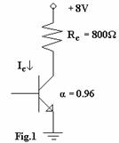
collector circuit is 0.5V. The value of Rc=800![]() . If
. If ![]() determine
determine
(i) Collector Emitter Voltage
(ii) Collector Current
(iii) Base Current amplification factor ![]()
(iv) Base Current
(v) Find the emitter Current (5)
b. State the regions of operation of a transistor and explain the biasing conditions for the three regions. (9)
c. What is the reverse saturation current? (2)
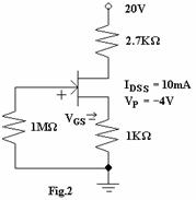
Q.4 a.
Draw the circuit diagram of a
b. What are the major differences between the collector characteristics of a BJT transistor and the drain characteristics of a JFET transistor? (3)
c. Determine ![]() and
and
![]() for the self-bias circuit shown in
Fig.2.
(9)
for the self-bias circuit shown in
Fig.2.
(9)
|
Q.5 a. State the Barkhausen conditions of oscillation in electronic system. What factors affect the frequency stability of an oscillator. (5)
b. (i) Calculate the
output voltage of an op-amp in both inverting and non-inverting configurations
when the input voltage is 10mV, ![]() and
and ![]() .
.
(ii) Design an amplifier with gain of –10. (6)
c. List the requirements of instrumentation amplifier and explain its working. (5)
Q.6 a.
Reduce the Boolean equation using Karnaugh
Map method ![]() and realise using basic
gates.
(4)
and realise using basic
gates.
(4)
b. Design and implement encoder using logic gates. (6)
c. Implement the X-OR function using only NOR gates. (6)
Q.7 a. Explain how active pull up is provided at the output of a TTL NAND gate with the help of a neat diagram. (5)
b. Explain the working of transmission gate as a Switch. (5)
c. Implement the following using CMOS logic
(i) NOR gate
(ii) XOR gate (6)
Q.8 a. Explain the race around condition in a JK flip flop. Explain the logic involved to prevent the race around condition with the help of a neat diagram. (8)
b. Design a mod 7 counter. (8)
Q.9 a. Define the terms Regulation and Peak inverse voltage in reference to rectifiers. (4)
b. Differentiate between EPROM and EEPROM. (6)
c. Discuss the architecture of programmable array logic. (6)