 Code: DE08
Subject: ANALOG ELECTRONICS
Code: DE08
Subject: ANALOG ELECTRONICS
Time: 3 Hours Max. Marks: 100
NOTE: There are 9 Questions in all.
· Question 1 is compulsory and carries 20 marks. Answer to Q. 1. must be written in the space provided for it in the answer book supplied and nowhere else.
· Out of the remaining EIGHT Questions answer any FIVE Questions. Each question carries 16 marks.
· Any required data not explicitly given, may be suitably assumed and stated.
Q.1 Choose the correct or best alternative in the following: (2x10)
a. In an ideal Op-amp, the input resistance is
(A) zero. (B) 100 ![]() .
.
(C) 200 ![]() . (D)
infinite.
. (D)
infinite.
b. The transistor is said to be in Q state, when
(A) no signal is applied to it. (B) it is unbiased.
(C) no current is flowing. (D)
![]() .
.
c. The minimum efficiency of class-B amplifier is
(A) 50%. (B) 78.5%.
(C) 25%. (D) 100%.
d. The negative feedback in amplifier is to
(A) decrease harmonic distortion. (B) decrease BW.
(C) increase voltage gain. (D) increase Power gain.
e. In an amplifier, a coupling capacitor is used to
(A) match the impedance. (B) prevent d.c. mixing with o/p.
(C) control frequency. (D) limit the bandwidth.
f. The voltage gain
of an amplifier is 100. When negative feedback with ![]() =0.04 is introduced, its
gain will be
=0.04 is introduced, its
gain will be
(A) 20. (B) 25.
(C) 4. (D) 0.4.
g. Both positive and negative feedback is employed in
(A) Hartley oscillator. (B) Colpitt's oscillator.
(C) Tuned collector. (D) Wien bridge oscillator.
h. Bandwidth of tuned circuit is given by
(A)
![]() . (B)
. (B)
![]() .
.
(C) ![]() . (D)
. (D)
![]() .
.
i. Stagger tuning is achieved by
(A) double tuned circuit.
(B) tuned circuits which are tuned to same frequency
(C) tuned circuits which are tuned to slightly different frequencies
(D) circuits tuned at harmonic frequencies
j. A bistable multivibrator has
(A) no stable state. (B) one stable state.
(C) two stable states. (D) alternate state ON/OFF.
Answer any FIVE Questions out of EIGHT Questions.
Each question carries 16 marks.
Q.2 a. Draw and describe the circuit diagram for collector to base resistor biasing. (8)
b. In a CE amplifier circuit, the following quantities are measured
(i) when ac output is short
circuited (i.e. ![]() )
)
![]()
(ii) when
ac input is opened (i.e. ![]() )
)
![]()
Determine the h-parameters of the amplifier circuit. (8)
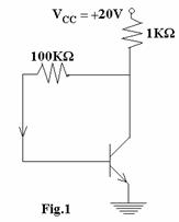
Q.3 a. As
shown in Fig.1 a silicon transistor biased by feedback resistor method.
Determine the operating point. Given that ![]() . (8)
. (8)
|
b. Draw the hybrid pi model for transistor in CE configuration and briefly explain the components of the model. (8)
Q.4 a. Explain the principle of negative feedback in amplifier and derive expression for gain of amplifier with negative feedback. (8)
b. The gain of amplifier without feedback is 100 where as with negative feedback it falls to 50. If due to ageing the amplifier gain falls to 80. Find the % reduction in stage gain
(i) without feedback. (ii) with negative feedback. (8)
Q.5 a. Draw the circuit diagram of transformer coupled class-A power amplifier and show that maximum collector efficiency for the circuit is 50%. (10)
|
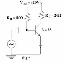
b. Calculate
(i) output power
(ii) input power
(iii) collector efficiency of the amplifier circuit shown in Fig.2. It is given that input voltage results in a base current of 10 mA peak. (6)
Q.6 a. What is a power amplifier? How it differs from a voltage amplifier? Why heat sinks are needed in power amplifiers? (8)
b. Draw the self bias circuit for n-channel JFET and explain how stabilization is achieved by this method. (8)
Q.7 a. Draw the circuit diagram of Colpitt's oscillator and explain its working. (8)
b. Explain briefly the Op-amp parameters. (8)
Q.8 a. Draw the circuit of an non-inverting amplifier using Op-amp and derive the equation for voltage gain. (8)
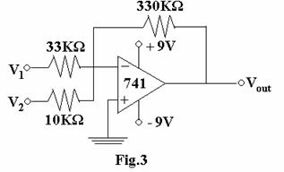
b. Find
the output voltage for the circuit given in Fig.3. The inputs are ![]() and
and ![]() . (8)
. (8)
|
Q.9 a. Determine the output voltage for the following circuits. Assume Ideal diode. . (8)
(i)

|
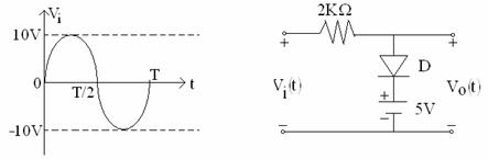
(ii)
b. Draw the circuit diagram of monostable multivibrator using 555 timer. (8)