 Code:
DE06 Subject:
BASIC ELECTRONICS
Code:
DE06 Subject:
BASIC ELECTRONICS
Time: 3 Hours Max. Marks: 100
NOTE: There are 9 Questions in all.
· Question 1 is compulsory and carries 20 marks. Answer to Q. 1. must be written in the space provided for it in the answer book supplied and nowhere else.
· Out of the remaining EIGHT Questions answer any FIVE Questions. Each question carries 16 marks.
· Any required data not explicitly given, may be suitably assumed and stated.
Q.1 Choose the correct or best alternative in the following: (2x10)
a. A 1000 ![]() capacitor is required for
an electronic circuit, such a large value of capacitance is possible if
capacitor is
capacitor is required for
an electronic circuit, such a large value of capacitance is possible if
capacitor is
(A) an Air-gang capacitor (B) a Mica capacitor
(C) An Electrolytic capacitor (D) a ceramic capacitor
b. An ideal voltage source of 12V provides a current of 150mA to a load. If the load resistance is tripled, the new load current becomes
(A) 150 mA (B) 75mA
(C) 50mA (D) 300mA
c. The depletion region of a semiconductor diode is due to
(A) reverse biasing (B) forward biasing
(C) crystal doping (D) migration of mobile charge carriers
d. The leakage current of a P-N junction diode is caused by
(A) chemical energy (B) heat energy
(C) barrier potential (D) majority carriers
e. When an NPN
transistor is cut-off, its ![]()
(A)
Equals
![]() and
and ![]() is high (B)
Equals
is high (B)
Equals ![]() and
and
![]() is
zero
is
zero
(C) is low and ![]() is high (D)
is high and
is high (D)
is high and ![]() is low
is low
f. FETs have similar properties to
(A) PNP transistors (B) NPN transistors
(C) thermionic valves (D) unijunction transistor
g. A Diac is equivalent to a
(A) Two inverse Parallel-connected SCRs with Common Gate
(B) Two inverse Parallel-connected SCRs without Common Gate
(C) diode and two resistors
(D) triac with two gates
h. An Ideal voltage regulator has a voltage regulation of
(A) 1 (B) 100
(C) 50 (D) 0
i. Op-amps have become very popular in industry mainly because
(A) they are dirt cheap
(B) their external characteristics can be changed to suit any application
(C) of their extremely small size
(D) they are available in different packages
j. The most popular form of IC package is
(A) Round To (Top-hat) – 05 package
(B) Flat package
(C) Dual-in-line plastic package
(D) Round To (Top-hat) –10 package
Answer any FIVE Questions out of EIGHT Questions.
Each question carries 16 marks.
Q.2 a. What is an AC voltage source? Draw its schematic representation and briefly explain its characteristics. Give two examples of AC voltage sources. (6)
b. What are the different types of fixed resistors? Explain their construction with the help of neat illustrations. Also give their resistance ranges and power ratings. (10)
Q.3 a. Explain why the conductivity of a pure semiconductor increases with temperature. When does an intrinsic semiconductor behave as an insulator? What is a hole in a semiconductor and how is it formed? (10)
b. Distinguish between Majority and Minority carriers in a semiconductor. What do you mean by mobility of charge carriers? (6)
Q.4 a. With the help of neat sketches, explain the working of a P-N junction in both forward and reverse biasing modes. Also plot the V-I characteristics. What is the cause of leakage current in reverse bias? (10)
b. Sketch the circuit diagram of a voltage Regular using a Zener diode and explain its working. Is there any limitation on the value of the series resistance used in this circuit? (6)
Q.5 a. Sketch a family of CE output characteristics for a transistor. Indicate the active, cutoff, and saturation point and explain the shapes of curves qualitatively. (8)
b. Discuss in detail the operation of Half wave and Full wave rectifier. (8)
Q.6 a. What is Bipolar junction transistor? Mention the
essential conditions required for transistor action. Prove that ![]() , where
, where ![]() and
and ![]() have their usual
meanings. (8)
have their usual
meanings. (8)
b. Give a table of comparison between Common Collector (CC) and Common Base (CB) configurations with regard to the important parameters. (4)
c. A
Germanium transistor with ![]() gives a reverse saturation current
gives a reverse saturation current ![]() , when used in
the Common Base configuration. When the transistor is connected in the Common
Emitter mode with a Base current of 0.2
, when used in
the Common Base configuration. When the transistor is connected in the Common
Emitter mode with a Base current of 0.2![]() , calculate the collector
current. (4)
, calculate the collector
current. (4)
Q.7 a. Explain with neat diagram, the construction and operation of N-channel JFET. What is the difference between N-channel JFET and P-channel JFET. (10)
b. What is a UJT? Explain its operation with the help of a circuit diagram. (6)
Q.8 a. Define the following terms used in IC fabrication:
(i) Chip (ii) Diffusion
(iii) Etching (6)
b. What is electron emission and mention different types of electron emissions? (6)
c. Write a note on Schottky diode. (4)
Q.9 a. What are the characteristics of an Ideal OP-AMP? (5)
b. In an inverting OP-AMP
shown in Fig.9(b),
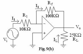
![]() ,
, ![]() ,
, ![]() and a load resistance of 25K
and a load resistance of 25K![]() is connected to
the output terminal. Calculate
is connected to
the output terminal. Calculate
(i)
Input current ![]() .
.
(ii)
Output Voltage ![]() and
and
(iii)
Load current ![]() (6)
(6)
c. Draw the circuit of voltage follower using OP-AMP and explain its operation. (5)