Code: DC02 Subject: FUNDAMENTALS OF ELECTRONICS
 Time:
3
Hours
Max. Marks: 100
Time:
3
Hours
Max. Marks: 100
NOTE: There are 9 Questions in all.
· Question 1 is compulsory and carries 20 marks. Answer to Q. 1. MUST BE WRITTEN IN THE SPACE PROVIDED FOR IT in the answer book supplied and nowhere else.
· Out of the remaining EIGHT Questions answer any FIVE Questions. Each question carries 16 marks.
· Any required data not explicitly given, may be suitably assumed and stated.
Q.1 Choose the correct or best alternative in the following: (2x10)
a. A resistor has a colour band sequence: grey, blue, gold and gold. Its value is
(A)
![]()
![]() 5% (B)
5% (B)
![]()
![]() 5%
5%
(C)
![]()
![]() 5%. (D)
5%. (D)
![]()
![]() 5%
5%
b. The resistance of an ac current source of strength 0.2A is 100![]() . Its equivalent
voltage source is
. Its equivalent
voltage source is
(A)
A
source of strength 15V in series with a resistance of 100![]()
(B)
A
source of strength 15V in shunt with a resistance of 100![]()
(C)
A
source of strength 20V in series with a resistance of 100![]()
(D) None of the above.
c. A device whose characteristics are very close to that of an ideal voltage source is
(A) A Photo diode (B) A field-effect transistor
(C) A transistor in CB mode (D) A Zener diode
d. If the reverse characteristic of a PN-junction diode shows a reverse current of one microampere at a voltage of 5 Volts, then the static resistance of the diode is
(A)
50 M![]() (B)
50 K
(B)
50 K![]()
(C) 5![]() (D)
5 M
(D)
5 M![]()
e. GaAs LEDs emits radiation in the
(A) Ultraviolet region
(B) Violet-blue green range of the visible region
(C) Visible region
(D) Infra-red region
f. In the logic circuit shown, the Boolean expression for the output X is
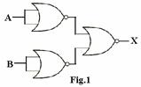
(A)
![]()
(B) A+B
(C) ![]()
(D) AB
g. Power is drawn by a CMOS circuit only when
(A) its output is high (B) its output is low
(C) it switches logic levels (D) in static state
h. Monolithic ICs are fabricated within a
(A) Metallic layer (B) Ceramic base
(C) Silicon layer (D) None of them
i. In the context of IC fabrication, metalisation means
(A) connecting metallic wires
(B) depositing SiO2 layer
(C) forming interconnecting conduction pattern and bonding pads
(D) covering with a metallic cap
j In the inverting amplifier circuit shown, if the OPAMP used in an ideal one, then the magnitude of the Voltage gain is
|

(A) 900
(B) 9000
(C) 1000
(D) 1200
Answer any FIVE Questions out of EIGHT Questions.
Each question carries 16 marks.
Q.2 a. How are electronic components classified? Give examples for each classification. (6)
b. For what type of resistors, a system of colour coding is used to indicate their values? Briefly explain the system of colour coding used in practice. (6)
c. A d.c. source has an open circuit voltage of 2V, and internal resistance of only one ohm. It is connected to a load resistance RL. The load resistance can assume any value ranging from one ohm to ten ohms. Find the variation in the terminal voltage of the source. (4)
Q.3 a. What is a semiconductor? What are its important properties? What do you mean by ‘doping’ as used in semiconductors theory and what is the use of a doped semiconductor? (7)
b. What is a PN junction? Draw the V-I characteristics of a PN-junction and briefly explain. How is static resistance of a diode defined? (9)
Q.4 a. What do you mean by Zener break down? Write the circuit symbol for a Zener diode. How is a Zener diode specified? (6)
b. The constant of proportionality between the capacitance of a Varactor diode and the reverse voltage applied is 36 x 10–12.
What will be the capacitance of the Varactor diode, when the reverse voltage applied across it is 4V? (4)
c. Which are the special purpose diodes used in electronic circuitry? (6)
Q.5 a. Compare CE, CB and CC configuration of BJT. (9)
b. What are the advantages of FETs over junction transistors? (4)
c. Comment on the use of FET as a switch. (3)
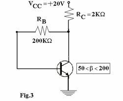
Q.6 a. What are
the requirements of a transistor biasing circuit? Calculate the minimum and
maximum collector current in the collector-to-base biasing circuit shown in
Fig.3, if the beta of the transistor varies within the limits indicated.
(9)
b. Illustrate the basic way of connecting the feed back signal in an amplifier with Voltage-shunt feedback and make the illustration self explanatory. In a negative feedback amplifier, the gain of the basic amplifier is 100 and the feedback factor is 0.04. If the input volt is 50mV, calculate
(i) the gain with feedback,
(ii) the output voltage of the amplifier and
(iii) the feedback voltage. (7)
Q.7 a. Prove the following using the basic laws and postulates of Boolean algebra: (i) X + X = X (ii) X + 1 = 1
Indicate the postulates used in each step of your proof. (6)
b. For the given Karnaugh map, write the minterm canonical expression. (3)
YZ
|
X |
|
|
|
|
||
|
|
1 |
0 |
0 |
1 |
||
|
|
1 |
1 |
0 |
0 |
c. Using a Karnaugh map, determine the prime implications of the Boolean function given below
![]() (7)
(7)
Q.8 a. Write in brief about the following of digital ICs:
(i) Noise Immunity (ii) Speed of operation (7)
b. Write the circuit of a two-input RTL NOR gate driving N similar gates and briefly explain the logic operation. Summarize the characteristics of RTL (9)
Q.9 a. Write the circuit of an OPAMP non-inverting amplifier and deduce the equation for the gain of the circuit. Based on its operation, can the above circuit be called by some other name? If yes, what is it? (6)
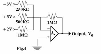
b. Find the output voltages of the OPAMP adder shown in Fig.4. (6)
|
c. Write a brief note on “resistance in monolithic circuits”. (4)