Flowchart: Alternate Process: DECEMBER 2008Code: AE27                                                               Subject: DIGITAL HARDWARE DESIGN

Time: 3 Hours                                                                                                     Max. Marks: 100


NOTE: There are 9 Questions in all.

·      Question 1 is compulsory and carries 20 marks. Answer to Q. 1. must be written in the space provided for it in the answer book supplied and nowhere else.

·      Out of the remaining EIGHT Questions answer any FIVE Questions. Each question carries 16 marks.

·      Any required data not explicitly given, may be suitably assumed and stated.


Q.1       Choose the correct or best alternative in the following:                                         (2x10)


a.       Output of NAND gate is high

(A) Only if both inputs are high

              (B) Only if both inputs are low

              (C) Only if one input is high and other is low

              (D) At least one of the inputs is low.


b.      The switching function


              can also be expressed as

              (A)                         (B)

              (C)                                                                             (D)


c.       The K-map method of minimization of switching function is very convenient and effective if numbers of variables in the switching function are

(A) 9                                                   (B) 10                                                                  

        (C) 4                                           (D) 8


d.   The logic gate to replace the logic circuit shown in figure is
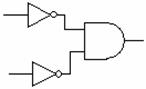


        (A) NAND                                 (B) NOR

        (C) XOR                                     (D) AND


e.    The maximum number of unique Boolean functions F (A,B), realizable for a two input  (A,B) and single output (Z) circuit is:


        (A) 4                                           (B) 6

(C) 8                                                   (D) 16

f.    A rectangular clock pulse has a frequency of 5MHz and width of positive pulse is 0.05μs. The high duty cycle will be

        (A) 25%                                      (B) 50%

        (C) 20%                                      (D) 15%


g.    How long will it take to shift an 8-bit number into a 54164(serial in parallel out) shift register if the clock is set at 10 MHz?

        (A) 1000 ns                                 (B) 100ns

        (C) 800 ns                                   (D) 8ms


h.    With respect to structural design style which of the following statement is true-

        (A) Circuit is described as a network of interconnected components.

        (B) This type of coding is non-synthesizable.

(C) Circuit is described using concurrent statements

(D) Most complicated form of coding.


i.     ______ are the unwanted pulses appearing at the output of a gate when two or more inputs change state simultaneously.

        (A) Clock                                    (B) Trigger pulses

        (C) Strobe pulses                        (D) Glitches


j.    The fundamental mode of operation of asynchronous sequential circuits is

        (A) Output change is based on change in the input level

        (B) Output toggles without change in input.

        (C) Output changes with external clock pulse.

        (D) Both input and output never change.


Answer any FIVE Questions out of EIGHT Questions.

Each question carries 16 marks.


  Q.2     a.   Minimize the Boolean functions with don’t care condition in

                   (i) Sum of product form                       (ii) product of sum form                         (12)


                   i.                         

                     ii.


             b.   Find the prime implicates of the function                                                              (4)


  Q.3     a.   Realize logic function  using only NOR gates.                          (4)


             b.   Compare –                                                                                                   (2x2)

                   (i)  Analog and digital signals

                   (ii) Combinational and sequential circuits


             c.   Write a VHDL – Structural design style code for 1-bit full adder.                        (8)


  Q.4     a.   Implement the following combinational circuits-                                              (4x2)

                   (i)  Full subtractor using two half subtractors and an OR gate.                                 

                   (ii) Full adder circuit with a 3x8 decoder and two OR gates.


             b.   Realize the following Boolean function using 4x1 MUX only.                               (8)


  Q.5     a.   What do you mean when you say ‘flip-flop is transparent’? With proper timing diagram for the flip-flops, define setup time, hold time, propagation delay.                                                                  (4)


             b.   Carryout following flip-flop conversions-                                                        (4x2)

                   (i)  RS flip-flop into T flip-flop

                   (ii) D flip-flop into T flip-flop                .                                                                 


             c.   List the different steps required for design of fundamental mode asynchronous sequential circuits.                                                               (4)


  Q.6     a.   Explain the components and organization of subsystem with example.                  (8)
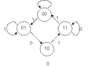
 

Text Box: 0             b.   For the state diagram shown in the figure, obtain the state table and design the circuit using minimum number of JK flip-flop                                      (8)


  Q.7     a.   What are the primary design constructs, or “Design Units”, used to describe logic in VHDL?                                                                     (4)


             b.   Explain in brief the commonly used modelling styles in VHDL?                           (4)


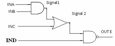
             c.   Write structural VHDL code for the logic circuit shown below-                          (8)


  Q.8     a.   Answer the following questions-                                                                     (4x2)

                   (i)What do you understand by explicit and implicit sequencing of microinstructions?

                   (ii)Discuss any two design related issues with asynchronous sequential circuits.


             b.   In how many ways the registers can store and retrieve binary information? List two applications of shift register                                                                                                              (6)


             c.   Explain Mealy and Moore machine                                                                     (2)


  Q.9           Write short notes on any FOUR                                                                     (4x4)

                   (i)   CPLD and FPGA

                   (ii)  Components of RTL data subsystems

                   (iii) ROM and its classification

                   (iv) MUX as Universal module

                   (v)  Priority encoder and binary decoders.