 Code:
AE05 Subject:
BASIC ELECTRONICS
Code:
AE05 Subject:
BASIC ELECTRONICS
Time: 3 Hours Max. Marks: 100
NOTE: There are 9 Questions in all.
· Question 1 is compulsory and carries 20 marks. Answer to Q. 1. must be written in the space provided for it in the answer book supplied and nowhere else.
· Out of the remaining EIGHT Questions answer any FIVE Questions. Each question carries 16 marks.
· Any required data not explicitly given, may be suitably assumed and stated.
Q.1 Choose the correct or best alternative in the following: (2x10)
a. In a p-type extrinsic semiconductor, the acceptor energy level is
(A) midway between valence and conduction band.
(B) nearer to valence band.
(C) nearer to the conduction band.
(D) within the conduction band.
b. For a doped semiconductor with free electron and hole concentrations
of n and p respectively and intrinsic carrier concentration of ![]() , the mass action
law is stated as:
, the mass action
law is stated as:
(A)
![]() (B)
(B)
![]()
(C) ![]() (D)
(D)
![]()
c. If the current
gains of transistors used in Darlington pair are ![]() and
and ![]() , the effective current gain of the
pair is
, the effective current gain of the
pair is
(A) ![]() (B)
(B)
![]()
(C) ![]() (D)
(D)
![]()
d. In an FET with ![]() = drain
resistance,
= drain
resistance, ![]() =
transconductance,
=
transconductance, ![]() Amplification factor, which of the
following statements is true?
Amplification factor, which of the
following statements is true?
(A)
![]() (B)
(B)
![]()
(C) ![]() (D)
(D)
![]()
e. An emitter follower can be used for
(A) capacitance transformation.
(B) impedance transformation.
(C) inductance transformation.
(D) applications where gain values of more than 10 are necessary.
f. When frequency stability is the main requirement one uses
(A) Colpitt oscillator (B) RC oscillator
(C) Hartley oscillator (D) Crystal oscillator
g. The slew rate of an Op-Amp is computed as
(A)
![]() (B)
(B)
![]()
(C) ![]() (D)
(D)
![]()
h. Rectification efficiency of a full-wave rectifier is about
(A) 81% (B) 61%
(C) 51% (D) 41%
i. When we apply
DeMorgan's theorem to the expression: ![]() we get
we get
(A)
![]() (B)
(B)
![]()
(C) ![]() (D)
(D)
![]()
|
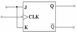
j. The figure shown represents
(A) D Flip-flop with –ve edge triggering.
(B) D Flip-flop with +ve edge triggering.
(C) JK Flip-flop with +ve edge triggering.
(D) T Flip-flop with –ve edge triggering.
Answer any FIVE Questions out of EIGHT Questions.
Each question carries 16 marks.
Q.2 a. Using clearly written figures, explain how DC and AC load lines are drawn on the V-I plane of a transistor in CE configuration. (10)
b. The reverse
saturation current of a transistor in CB configuration is 12![]() Calculate its collector
current when it is used in CE configuration with a base drive of 0.25
Calculate its collector
current when it is used in CE configuration with a base drive of 0.25![]() if its
if its ![]() . (6)
. (6)
Q.3 a. Draw hybrid parameter equivalent circuit of common emitter transistor amplifier and derive the expressions for current gain, voltage gain, input impedance and output impedance. (10)
b. Draw circuit diagram of Darlington amplifier. Give its main characteristics, merits and applications. (6)
Q.4 a. Describe the structure of JFET and explain 'pinch off' in the device. (9)
b. Find the
transconductance value of a JFET having ![]() and
and ![]() . (7)
. (7)
Q.5 a. Draw the circuit of a class-B push-pull amplifier using complementary symmetry transistors and explain its operation. (8)
b. Explain by mathematical analysis, how the bandwidth of an amplifier is extended by negative feedback. (8)
Q.6 a. Draw the circuit diagram of a phase-shift oscillator and describe its operation. (8)
b. Show the block schematic of typical Op-Amp and explain the function of each block. (8)
Q.7 a. Draw the circuit of a monostable multivibrator using two transistors and explain its operation with reference to waveforms of pertinent node voltages in the circuit. Analyze the circuit to obtain an expression for the pulse period. (10)
b. Show how a timer IC 555 can be used for generation of ramp waveforms. (6)
Q.8 a. Show a circuit scheme of a complete power supply using a suitable voltage regulator IC for DC supply of 12V. Clearly indicate the component values proposed by you. (8)
b. Define ripple factor in a basic rectifier. Explain the necessity to use filters in conjunction with rectifiers. (4)
c. Explain application of Op-Amp as a summer. (4)
Q.9 a. Draw the logic diagrams of
(i) 4 to 1 multiplexer (ii) 1 to 4 demultiplexer.
and explain their operation bringing out their reciprocal roles. (8)
b. What is edge triggering in flip-flops? Why it is preferred against level triggering? Construct a 4-bit binary synchronous UP counter using T flip-flops and describe its operation. (8)