 Code: AC03/AT03 Subject:
BASIC ELECTRONICS &
Code: AC03/AT03 Subject:
BASIC ELECTRONICS &
Time: 3 Hours DIGITAL CIRCUITS
Max. Marks: 100
NOTE: There are 9 Questions in all.
· Question 1 is compulsory and carries 20 marks. Answer to Q. 1. must be written in the space provided for it in the answer book supplied and nowhere else.
· Out of the remaining EIGHT Questions answer any FIVE Questions. Each question carries 16 marks.
· Any required data not explicitly given, may be suitably assumed and stated.
Q.1 Choose the correct or best alternative in the following: (2x10)
a. The mobility of
electrons in an N-type semiconductor is ![]() . If the resistivity of the
semiconductor is
. If the resistivity of the
semiconductor is ![]() , then the number of electron
carriers per
, then the number of electron
carriers per ![]() will
be,
will
be,
(A)
![]() . (B)
. (B) ![]() .
.
(C) ![]() . (D)
. (D)
![]() .
.
|
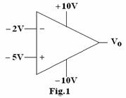
b. The output of comparactor is
(A) –2 V
(B) –5 V
(C) +10 V
(D) –10 V
c. Which of the following h-parameters of a transistor has the greatest value
(A)
![]() (B)
(B)
![]()
(C)
![]() (D)
(D)
![]()
d. If
the value of ![]() for the two transistors used in a Darlington amplifier are 150 and 100 respectively, then the overall current gain of the
amplifier is
for the two transistors used in a Darlington amplifier are 150 and 100 respectively, then the overall current gain of the
amplifier is
(A) 14000. (B) 12000.
(C) 15000. (D) 1000.
e. The
parameters of a JFET used in a common source amplifier are : ![]() and
and ![]() . If the value of
the load in the drain circuit is 10
. If the value of
the load in the drain circuit is 10![]() , then the voltage gain for the
amplifier is
, then the voltage gain for the
amplifier is
(A) –14.5. (B) 52.5.
(C) –100. (D) –24.5.
|
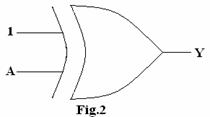
f. The output Y of Logic circuit is
(A) 0
(B) 1
(C) ![]()
(D) ![]()
g. The complement of
the Boolean expression ![]() is
is
(A)
A+BC (B)
![]()
(C) ![]() (D)
1
(D)
1
h. When ![]() is subtracted
from
is subtracted
from ![]() using
2’s complement method, the result is
using
2’s complement method, the result is
(A)
![]() . (B)
. (B)
![]() .
.
(C) ![]() . (D)
. (D)
![]() .
.
i. The fastest Logic family is
(A) TTL (B) CMOS
(C) ECL (D) HTL
j. How many address
bits are needed to operate a ![]() - bit ROM memory?
- bit ROM memory?
(A) 8 (B) 15
(C) 32 (D) 11
Answer any FIVE Questions out of EIGHT Questions.
Each question carries 16 marks.
Q.2 a. What is a semiconductor? How does a semiconductor behave at absolute zero temperature? Name four semiconductor materials. (6)
b. Design a 4-bit serial-in parallel out Left shift Register. (5)
|
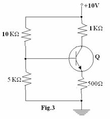
c. Determine the value of the collector
current and collector-to-emitter voltage
for the voltage divider of biasing
for the transistor shown in Fig.3.
Take
![]() and
and ![]() for
for
the transistor used. (5)
Q.3 a. Describe the advantages of h-parameters? Draw
Low frequency small signal hybrid-model for a common emitter transistor and determine
Voltage gain (![]() ),
Current gain
),
Current gain ![]() ,
Input Impedance
,
Input Impedance ![]() and
Output Impedance
and
Output Impedance ![]() .
(12)
.
(12)
b. For the amplifier circuit
shown in Fig.4, write the h-parameter equivalent circuit and find the current
gain for the amplifier. The transistor h-parameters are:
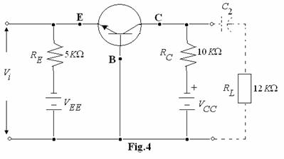
![]()
![]() . (4)
. (4)
Q.4 a. Draw the a.c. equivalent circuit of a JFET common-drain amplifier and derive the voltage gain of the amplifier. (8)
b. Draw the circuit diagram
of RC phase oscillator and derive the condition for oscillation. Neglect the
effects of ![]() and
and ![]() . (8)
. (8)
Q.5 a. Draw the circuit of basic Integrator and differentiator using an op-Amp and explain its operation. (6)
b. Calculate
the output voltage for the circuit given in Fig.5. The input voltages are
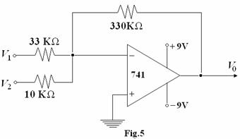
![]() and
and
![]() . (5)
. (5)
c. What do you mean by a Regulated Power Supply? What are the important elements of a regulated Power supply? Define the term Voltage Regulation. (5)
Q.6 a. Prove the following: ![]() . (5)
. (5)
b. Minimize the Boolean expression given using K-map method.
![]() (6)
(6)
c. Write the truth table and logic diagram of 1:8 demultiplexer; using NAND gates only. (5)
Q.7 a. What is a Schottky diode? Comment on the storage time of Schottky diodes. (6)
b. Explain NMOS logic circuit? Draw the circuit of an NMOS inverter that uses an n-channel enhancement-type MOSFET as a load resistor and briefly explain its operation. (10)
Q.8 a. What is ECL? Mention its characteristics. (8)
b. Write a note on programmable logic arrays. (8)
Q.9 a. Draw a static CMOS memory cell and explain it’s read and write operations. (6)
b. What do you mean by ‘STATE’ of a counter? Draw the schematic of a four-bit synchronous binary UP-Counter using T flip-flops (positive edge triggered) and briefly explain it. (10)
 |